I have spent some time this week thinking about a lab for characterizing nFETs (and pFETs) for the applied electronics course, because I was not very happy with the preliminary work in Possible new FET lab for electronics course and pFET Ron_vs_Vgs. There were a couple of things that bothered me:
- Should we be looking at equivalent resistance or current? which is more consistent across different test conditions? which is more useful for continued design?
- Does it matter what circuit we use for making the measurement? What are the advantages or disadvantages of choosing different power supply values, different load resistors, or different transistor configurations?
The most basic choice is between a common-source or common-drain amplifier setup, both of which are special cases of the same circuit:

For a common-source configuration, the output is Vd, the load resistor is Rd, and Rs is set to 0Ω. For a common-drain configuration, Vs is the output, Rs is the load resistor, and Rd is set to 0Ω.
The testing I did before was with a common-source circuit. The output voltage range is from very close to 0V up to Vdd, which means that either Vdd has to be limited to the range of the analog-to-digital converter or a voltage divider is needed to divide down Vd. The current we are interested in is 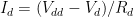
The common-drain circuit only requires measuring Vg and Vs, both of which can be within the analog-to-digital converter range even when Vdd is large, assuming that the load resistor (Rs in this case) is chosen sufficiently small. Determining Vgs requires a subtraction, but Id does not. Avoiding voltage dividers (with their current stealing and the extra trouble of measuring the divider ratio) seemed like a good idea.
I tried making measurements with the common-drain configuration today, and found it surprisingly difficult. I kept getting huge amounts of noise on the Vs plot, whenever the FET was on. It appeared to be 120Hz interference, but I have no idea where the interference was coming from—the power supply did not show significant 120Hz ripple and large bypass capacitors on the power supply lines did not help. I finally managed to get rid of the problem by putting a 10µF capacitor between the source and drain, providing a negative feedback path that eliminated the problem. (The capacitor appeared to make no difference to the plots for common-source configurations.)
The common-source circuits, however, provided much cleaner plots than the common-drain circuits. The common-source circuits also allowed me to measure much higher drain currents, because I could go to a higher Vgs value without exceed the ADC range when Vs was constrained to be 0V.
For the range that I could measure, I got essentially the same current whether I measured drain current or source current, and pretty much independent of the voltage and load resistance I used. To first approximation, it looks like Id is a function of Vgs in a way that the equivalent resistance that plotted in Possible new FET lab for electronics course is not.

Using a small load resistor allows measuring up to a fairly high current (Vdd/R), as long as the power supply can deliver the current and the resistor doesn’t overheat. Using a large load resistor allows measuring to a fairly low current.

")
 or hardback ($198)")


[…] week (or more) about why my FET measurements in Possible new FET lab for electronics course, , More thoughts on measuring FETs, and Measuring a high-voltage nFET were not coming out the way I expected. In particular, I was […]
Pingback by Why my nFET measurements were bad | Gas station without pumps — 2016 July 31 @ 22:53 |