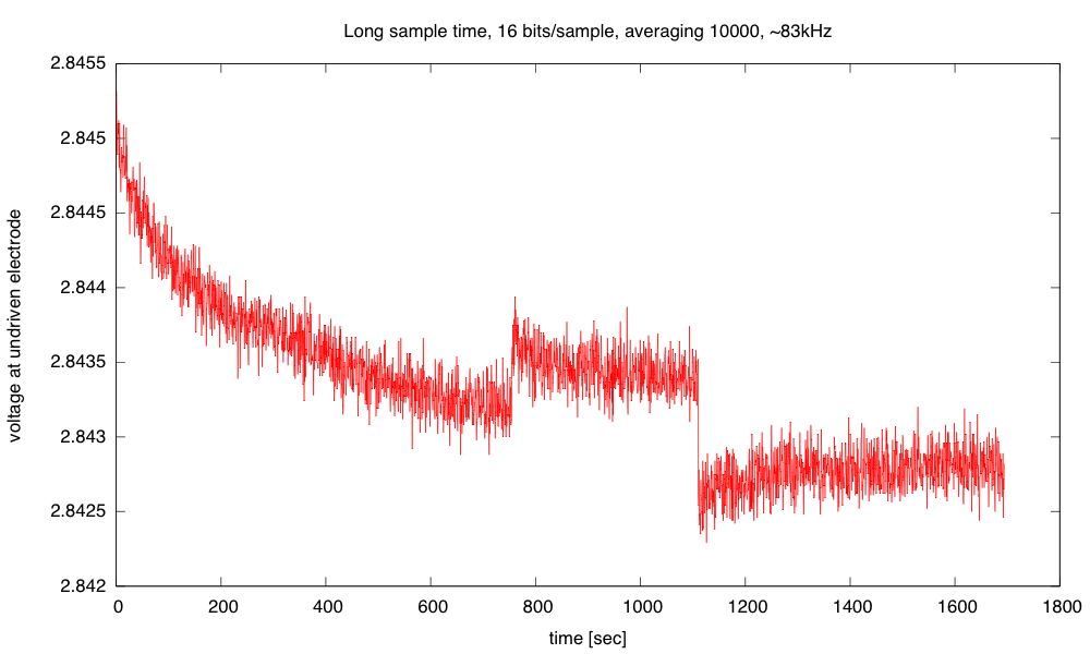
I was curious what the range of voltage measurements would be for different salt concentrations, and how linear the measurements would be. Measurements were made with a modified program, so that I could measure the applied voltage at the drive electrode as well as the voltage at the sense electrode. Conductance was computed as 0.01S * V_resist / (V_applied – V_resist).
| solution | V applied | V resist | conductance |
|---|---|---|---|
| distilled | 3298.1mV | 1.93±0.08mv | 5.86µS |
| tap water | 3257.4mV | 424.80±0.14mV | 1.50mS |
| 0.1M NaCl | 3074.0mV | 2265.31±0.15mV | 28.01mS |
| 1.0M NaCl | 3012.4mV | 2842.13±0.09mV | 166.9mS |
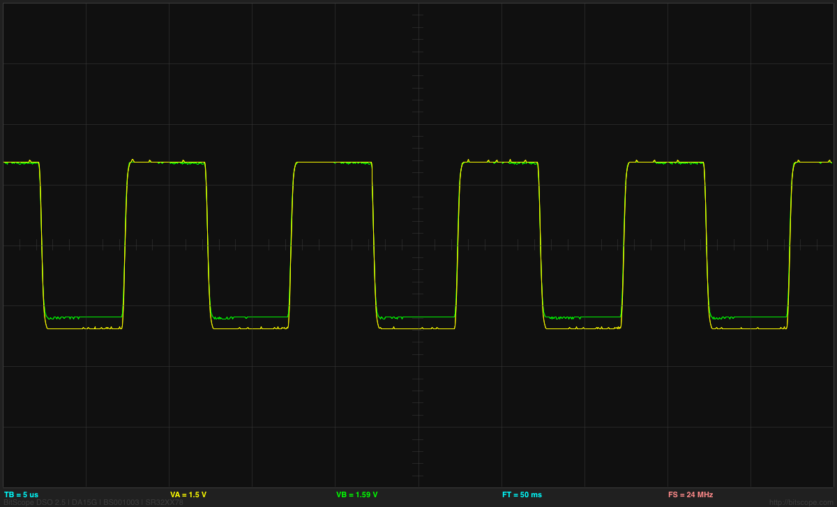
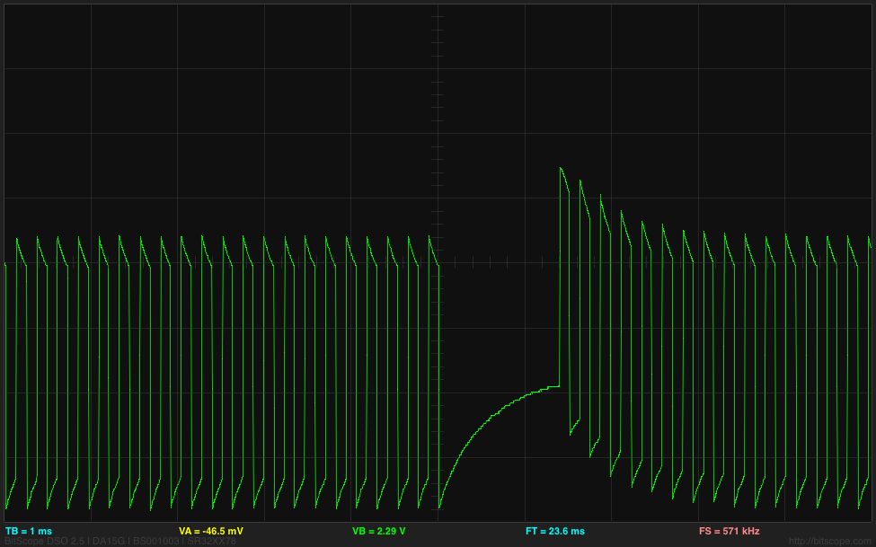
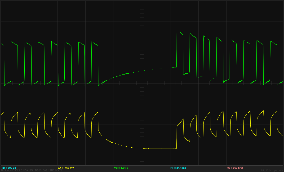
The first version of the program seemed to have some problems with fluctuation in the period of the square wave, probably from using the same pin for both digital out and analog in. I hooked up another pin to monitor the digital output and got a more consistent 65kHz square wave.
Repeating the measurements got me
| solution | V applied | V resist | conductance |
|---|---|---|---|
| distilled | 3297.71±0.12mV | 9.73±0.18mV | 29.59µS |
| tap water | 3258.75±0.07mV | 415.10±0.25mV | 1.46mS |
| 0.1M NaCl | 3065.05±0.08mV | 2271.82±0.23mV | 28.64mS |
| 1.0M NaCl | 3000.60±0.24mV | 2850.30±0.24mV | 189.6mS |
The small differences are probably from cross contamination as I moved the electrodes from one bath to another. I wiped them between measurements, but did not get them completely clean and dry.
The 0.1M and 1.0M solutions do not show a ten-fold ratio of conductances, only about 6–6.6 depending which set of measurements one takes. Either I did the dilution to make the 0.1M solution wrong (quite possible—I’m clumsy at even trivial wet-lab stuff) or my assumption that conductance should be linear with concentration is way off. It looks like the device should be able to measure from about 1E-4M to 3M NaCl. There is enough resolution in the ADC measurements to go down to 1E-5M (if the electrodes could avoid contaminating that) and up to saturated salt (about 6.2M). It would be important to have a series of test solutions to calibrate the unit, if the linearity assumption is wrong.
Here is a plot of the ionic concentration vs time for the second set of readings, based on the assumption of linearity and the correctness of the 1MNaCl reading:

Concentration is calculated as V_resist/(V_applied–V_resist) /18.96
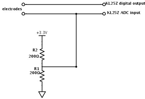
Here is the source code for the KL25Z (using the mbed.org compiler). Pins A0 and A2 were connected to the drive electrode, pin A1 to the sense electrode.
The sense electrode electrode was connected via 200Ω resistors to Gnd and 3.3V.
#include "mbed.h"
Serial USB_io(USBTX, USBRX); // defaults to 9600 8N1 (reset in main to 115200 baud)
Timer since_start;
AnalogIn Vapply(PTB2);
AnalogIn Vsense(PTB1);
DigitalInOut square_out(PTB0); // PTB0=arduino A0
//PTB0, PTB1, PTD6, and PTD7 I/O have both high drive and normal drive capability selected by the associated PTx_PCRn[DSE] control bit.
#define WARMUP (20000) // number of cycles of toggling output before collecting data
#define COLLECT (10000) // number of cycles of data to sum for each output
#define Vdd (3.3) // High voltage at output
int main()
{
USB_io.baud(115200);
USB_io.printf("\nusec\tV_out\tV_appl\nN\tN\tN\n");
//DEFAULT configuration of analog input
ADC0->CFG1 = ADC_CFG1_ADLPC_MASK // Low-Power Configuration
| ADC_CFG1_ADIV(3) // Clock Divide Select: (Input Clock)/8
| ADC_CFG1_ADLSMP_MASK // Long Sample Time
| ADC_CFG1_MODE(3) // (16)bits Resolution
| ADC_CFG1_ADICLK(1); // Input Clock: (Bus Clock)/2
ADC0->CFG2 = ADC_CFG2_MUXSEL_MASK // ADxxb channels are selected
| ADC_CFG2_ADACKEN_MASK // Asynchronous Clock Output Enable
| ADC_CFG2_ADHSC_MASK // High-Speed Configuration
| ADC_CFG2_ADLSTS(0); // Long Sample Time Select
ADC0->SC2 = ADC_SC2_REFSEL(0); // Default Voltage Reference
ADC0->SC3 = ADC_SC3_AVGE_MASK // Hardware Average Enable
| ADC_SC3_AVGS(0); // 4 Samples Averaged
// FAST analog input
// SIM->SCGC6 |= SIM_SCGC6_ADC0_MASK; // enable ADC0 clock
// SIM->SCGC5 |= 1 << (SIM_SCGC5_PORTB_SHIFT); // enable PORTB clock
ADC0->SC1[1] = ADC_SC1_ADCH(ADC0_SE9); // PTB1
ADC0->CFG1 =
ADC_CFG1_MODE(3) // (16)bits Resolution
| ADC_CFG1_ADLSMP_MASK // Long Sample Time
| ADC_CFG1_ADICLK(0); // Input Clock: (Bus Clock)
ADC0->CFG2 = ADC_CFG2_MUXSEL_MASK // ADxxb channels are selected
| ADC_CFG2_ADACKEN_MASK // Asynchronous Clock Output Enable
| ADC_CFG2_ADHSC_MASK // High-Speed Configuration
| ADC_CFG2_ADLSTS(0); // longest "long" Sample Time Select
// | ADC_CFG2_ADLSTS(3); // shortest "long" Sample Time Select
ADC0->SC2 = ADC_SC2_REFSEL(0); // Default Voltage Reference
ADC0->SC3 = 0; // No hardware averaging
// PTB1 and PTB2 set as analog inputs
// PORTB->PCR[1] = 0;
// PORTB->PCR[2] = 0;
// set PORTB pin 0 to high drive here
PORTB->PCR[0] |= PORT_PCR_DSE_MASK;
since_start.start();
while(1)
{ wait_us(100);
square_out.output();
int32_t sum_in=0;
int32_t sum_out=0;
for (int i=0; i
{
square_out=1;
wait_us(1);
ADC0->SC1[0] = ADC_SC1_ADCH(ADC0_SE9); // PTB1
// Wait Conversion Complete
while ((ADC0->SC1[0] & ADC_SC1_COCO_MASK) != ADC_SC1_COCO_MASK);
int32_t in_read=ADC0->R[0];
ADC0->SC1[0] = ADC_SC1_ADCH(ADC0_SE12); // PTB2
// Wait Conversion Complete
while ((ADC0->SC1[0] & ADC_SC1_COCO_MASK) != ADC_SC1_COCO_MASK);
int32_t out_read=ADC0->R[0];
square_out=0;
wait_us(1);
ADC0->SC1[0] = ADC_SC1_ADCH(ADC0_SE9); // PTB1
// Wait Conversion Complete
while ((ADC0->SC1[0] & ADC_SC1_COCO_MASK) != ADC_SC1_COCO_MASK);
sum_in += in_read - ADC0->R[0];
ADC0->SC1[0] = ADC_SC1_ADCH(ADC0_SE12); // PTB2
// Wait Conversion Complete
while ((ADC0->SC1[0] & ADC_SC1_COCO_MASK) != ADC_SC1_COCO_MASK);
sum_out += out_read - ADC0->R[0];
}
sum_in=0;
sum_out=0;
for (int i=0;i<COLLECT; i++)
{
square_out=1;
wait_us(1);
ADC0->SC1[0] = ADC_SC1_ADCH(ADC0_SE9); // PTB1
// Wait Conversion Complete
while ((ADC0->SC1[0] & ADC_SC1_COCO_MASK) != ADC_SC1_COCO_MASK);
int32_t in_read=ADC0->R[0];
ADC0->SC1[0] = ADC_SC1_ADCH(ADC0_SE12); // PTB2
// Wait Conversion Complete
while ((ADC0->SC1[0] & ADC_SC1_COCO_MASK) != ADC_SC1_COCO_MASK);
int32_t out_read=ADC0->R[0];
square_out=0;
wait_us(1);
ADC0->SC1[0] = ADC_SC1_ADCH(ADC0_SE9); // PTB1
// Wait Conversion Complete
while ((ADC0->SC1[0] & ADC_SC1_COCO_MASK) != ADC_SC1_COCO_MASK);
sum_in += in_read - ADC0->R[0];
ADC0->SC1[0] = ADC_SC1_ADCH(ADC0_SE12); // PTB2
// Wait Conversion Complete
while ((ADC0->SC1[0] & ADC_SC1_COCO_MASK) != ADC_SC1_COCO_MASK);
sum_out += out_read - ADC0->R[0];
}
square_out.input(); // hiZ state when not driving pulses
USB_io.printf("%10d\t%7.5f\t%7.5f\t\n", since_start.read_us(), sum_in*(Vdd/COLLECT/(1<<16)),sum_out*(Vdd/COLLECT/(1<<16))); // scale output to volts
}
}
 , where Z is the impedance of the electrodes (which varies with frequency) and R is the known resistance.
 , so
, so  .
.


")
 or hardback ($198)")

