Gas station without pumps

2014 July 3

Digital filters: infinite-impulse-response filters

Filed under: Uncategorized — gasstationwithoutpumps @ 17:13
Tags: , , , , , ,

Yesterday I wrote a very brief introduction to z-transforms and finite-impulse-response filters.  Today I’ll try to do infinite-impulse-response (IIR) filters.  Obviously, one blog post can’t do justice to the topic, but I’ll try to get far enough that my son can implement some simple filters for his project.  If he needs more detail, the tutorial at CCRMA by Julius Smith is probably worth reading.

The basic idea of an IIR filter is that the transfer function is not a polynomial but a rational function.  For example, the standard “biquad” digital filter unit is the ratio of two quadratic formulas: H(z) = \frac{b_{0} + b_{1}z^{-1} + b_{2}z^{-2}}{1 + a_{1}z^{-1} + a_{2}z^{-2}}.

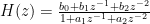
There are a lot of different ways to implement the biquad section, trading off various properties, but one that has particularly nice numeric properties is the “direct form I” implementation.

Direct form I for implementing a biquad filter section.  Taken from https://ccrma.stanford.edu/~jos/filters/Direct_Form_I.html

Direct form I for implementing a biquad filter section. Taken from https://ccrma.stanford.edu/~jos/filters/Direct_Form_I.html

The transfer function can be checked by looking at the summation in the center and taking z-transforms: Y(z) = X(z)(b_{0} + b_{1}z^{-1} + b_{2}z^{-2}) - Y(z)(a_{1}z^{-1} + a_{2}z^{-2}), followed by simple algebra to rearrange to get the transfer function above. One nice property of this particular implementation for fixed-point computation is that as long as the output stays within range, there are no problems with overflow in intermediate computations.

The left half of the implementation computes the numerator of the transfer function, which may have either two real zeros or a conjugate pair of complex ones (or a single real zero, if b2=0).  It is often useful to look at these zeros in polar form, Ae^{i\theta}, since the resulting filter will have minima at \omega=\theta, and how sharp the minimum is depends on how close A gets to 1. One popular choice for bandpass filters is to put the zeros at 1 and –1, so that there are zeroes at DC (ω=0) and at the Nyquist frequency (ω=π), which gives 1-z^{-2} as the numerator. For a low-pass filter, both zeros are often put at the Nyquist frequency, giving (1+z^{-1})^2, while for a high-pass filter, both zeros are often put at DC, giving (1-z^{-1})^2.

The right half of the implementation computes the denominator of the transfer function producing a pair of poles, and it is again useful to look at the poles in polar form. For stability of the filter we need to have the poles within the unit circle— even getting them too close to the unit circle can cause the output to get very large and cause numeric overflow.

Note that any rational function with real coefficients can be factored into biquad units with real coefficients, just by factoring the polynomials into a product of roots, and pairing the complex roots in their conjugate pairs. Because the direct implementation of a high degree polynomial is very sensitive to rounding errors in the parameters, it is common to factor the transfer function into biquad units.

About a year ago, I was playing with a biquad filter for an optical pulse monitor, where I wanted a roughly 0.4—2.5 Hz bandpass filter, with a sampling rate of 30Hz, using only small integer coefficients. I put the zeros at 1 and —1, and used a filter-design site on the web to get real-valued coefficients for the denominator. I then approximated the real-valued coefficients as integers divided by powers of two, and tried tweaking the coefficients up and down to get close to the response I wanted, using gnuplot to plot the gain:

Biquad design for a bandpass filter with peak around ω=π/15 using only small integer coefficients.

Biquad design for a bandpass filter with peak around ω=π/15 using only small integer coefficients.

The code I used for implementing the biquad bandpass filter on a microcontroller was fairly simple:

     y_0 = b0*(x_0-x_2) - a1*y_1 -a2*y_2;
     Output(y_0);
     x_2 = x_1;
     x_1 = x_0;
     y_2 = y_1;
     y_1 = y_0/a0;

Note that I’m outputting the high-precision output from the summation node, which has an extra gain of a0. The memory elements (x_1, x_2, y_1, y_2) have the same precision as the input—only the summation is done at higher precision. The division in the last line is not really a division but a shift, since I restricted a0 to be a power of 2. This shifting could be done after the multiplications of y_1 and y_2 in the first line, if y_1 and y_2 are carried to higher precision, but then the intermediate results in the summation could get too large—a lot depends on how big the word size is compared to the input values and the a0 scaling.

My son is probably interested in two digital filters—one to remove the DC bias (so a high-pass with cutoff frequency around 10–20Hz) and one to pick out the beat from a non-linearly modified signal (absolute value or squared signal). The beat he is interested in picking out is probably around 60–180bpm or 1–3Hz—similar to what I did for picking out heartbeats (I used 0.4—2.5Hz as a rough design goal on the pulse monitor). Unfortunately, as you go to higher sampling frequencies, you need to have higher precision in the filter coefficients.

The biquad coefficient calculator at http://www.earlevel.com/main/2013/10/13/biquad-calculator-v2/ seems pretty good, though it is a bit tedious to rescale and round the coefficients, then check the result. So I wrote a Python script to use the scipy.signal.iirfilter function to design filters, then scaled and rounded the coefficients. The scaling factor had to get much larger as the sampling frequency went up to get a good bandpass filter near 1Hz, otherwise rounding errors resulted in a low-pass filter rather than a bandpass filter (perhaps one of the poles ended up at 1 rather than as a complex pair?). To make a 0.33–3Hz bandpass filter, I needed to scale by 230 at 40kHz, 221 at 10kHz, 216 at 3kHz, 215 at 1kHz, 211 at 300Hz, and 28 at 100Hz. The scaling factors needed for 40kHz sampling would exceed the 32-bit word size, so this approach did not look very promising.

It may be more effective to use two separate biquad sections: a low-pass filter with a fairly high cutoff to downsample the signal, then a bandpass filter at the lower sampling rate. This approach allows using much lower-precision computations. I wrote a little Python program to test this approach also, aiming for a 0.33–3Hz bandpass filter.

Here is the filter response of a low-pass filter, followed by down-sampling and a bandpass filter.  Note that the scaling factor is only 2 to the 14, but the  filter response is quite nice.

Here is the filter response of a low-pass filter, followed by down-sampling and a bandpass filter. Note that the scaling factor is only 214, but the filter response is quite nice.

So the overall design of the loudness sensor will probably be a series of filters:

  • high-pass filter at 20Hz to remove DC bias, leaving sound
  • nonlinear operation (squaring or absolute value)
  • low-pass filter at 200Hz
  • down-sample to 500Hz
  • bandpass filter at 0.33–3Hz

One possible problem with this approach—look at the phase change when the beat is not 1Hz. At 0.33Hz, the phase change is about 37º, which is about 0.3s—a larger shift in the beat than we’d want to see. We may have to look at more complicated filter design that has smaller phase shifts. (The -49º phase shift at 3Hz is only about 45msec, and so not a perceptual problem.)

Here is a possible filter design for the initial high-pass filter:

Getting a 20Hz cutoff frequency required a somewhat larger scaling factor than for the other filters, but still quite reasonable for 14-bit values on a 32-bit machine.

Getting a 20Hz cutoff frequency required a somewhat larger scaling factor than for the other filters, but still quite reasonable for 14-bit values on a 32-bit machine.

Here is a version of the two-stage filter design program:

#!/usr/bin/env python

from __future__ import division,print_function

import numpy as np
import scipy
from scipy.signal import iirfilter,freqz,lfilter,tf2zpk
import matplotlib.pyplot as plt

pi=3.1415926535897932384627

fs = 40.e3  # sampling frequency

low_fs = 1000.  # sampling frequency after downsampling
cutoffs = (0.33,3.0)  # cutoff frequencies for bandpass filter in Hz

scale_factor = 2.**14

def scaled(b,a):	
    """scaled b and a by scale_factor and round to integers.
    Temporarily increase scale factor so that b[0] remains positive.
    """
    extra_scale=1.
    b_scaled = [int(np.round(scale_factor*c*extra_scale)) for c in b]
    while b_scaled[0]==0:
        b_scaled = [int(np.round(scale_factor*c*extra_scale)) for c in b]
        extra_scale *= 2
    a_scaled = [int(round(scale_factor*c*extra_scale)) for c in a]
    
    print (" b=",b, "a=",a)
    z,p,k = tf2zpk(b,a)
    print ( "zeros=",z, "poles=",p, "gain=",k)

    print ("scaled: b=",b_scaled, "a=",a_scaled)
    z,p,k = tf2zpk(b_scaled,a_scaled)
    print ( "zeros=",z, "poles=",p, "gain=",k)        

    return b_scaled,a_scaled    


def plot(b1,a1, b2,a2, frequencies=None):
    """Plot the gain (in dB) and the phase change of the
    concatentation of filters sepecified by b1,a1 and b2,a2.
    
    The b1,a1 filter is designed to run at sampling rate fs
    
    The b2,a2 filter is designed to run at sampling rate low_fs
    
    Both are designed with the filter type specified in global filter.
    """

    if frequencies is None:
    	worN =[pi*10.**(k/200.) for k in range(-1000,0)]
    else:
    	worN = [2*pi*f/fs for f in frequencies]
        
    freq,response1 = freqz(b1,a1, worN=worN)
    freq2,response2 = freqz(b2,a2, worN=[f*fs/low_fs for f in worN])
    freq *= fs/(2*pi)

    response = response1*response2
    
    fig=plt.figure()
    plt.title ('{}: b1={} a1={} fs={}\n b2={} a2={} fs={}'.format(filter,b1,a1,fs,b2,a2,low_fs))

    ax1 = fig.add_subplot(111)
    plt.semilogx(freq,20*np.log10(np.abs(response)), 'b')
    plt.ylabel('Amplitude [dB]', color='b')
    plt.grid()
    plt.legend()
    plt.xlabel('Frequency [Hz]')

    ax2 = ax1.twinx()
    angles = [ 180/pi*ang for ang in np.unwrap(np.angle(response)) ]
    plt.plot(freq,angles, 'g')
    plt.ylabel('Phase change [degrees]', color='g')
    plt.show()        


for low_fs in [100., 200., 400., 500., 800., 1000., 2000.]:
    filter='bessel'
    low_cut = 0.4*low_fs
    b1,a1 = iirfilter(2, low_cut/fs, btype='lowpass', ftype=filter, rp=0.1, rs=0.1)
    print (filter, "lowpass for fs=",fs, "cutoff=", low_cut)
    b1_scaled,a1_scaled = scaled(b1,a1)

    b2,a2 = iirfilter(1, [2*f/low_fs for f in cutoffs], btype='bandpass', ftype=filter, rp=0.1, rs=0.1)
    print(filter, "bandpass for fs=", low_fs, "cutoffs=",cutoffs)
    b2_scaled,a2_scaled = scaled(b2,a2)

    plot(b1_scaled, a1_scaled, b2_scaled, a2_scaled, [10.**(k/200.) for k in range(-400,min(401,int(200.*np.log10(low_fs/2))))])

2014 February 8

More on loudness circuits

Filed under: Circuits course — gasstationwithoutpumps @ 21:07
Tags: , , , ,

My son got interested in a loudness circuit again, and we tried coming up with one that that would take few components. We decided on having a 3-stage system: a preamp to get voltage up, a peak (or trough) detector with low-pass filter to extract the envelope, and a log amplifier to convert to a dB scale. We were planning to use a Schottky diode, rather than a precision rectifier for the peak detector.

Block diagram for loudness sensor using peak detector.

Block diagram for loudness sensor using peak detector.

The gain of the first stage was set by looking at the sensitivity of the SPU0410HR5H‐PB silicon microphone and the maximum loudness that the system should be able to record. The mic has -42±3dB sensitivity referenced to 1V/Pa.  That means it has 7.94mV/Pa.  The loudest sound for the mic should be the sound level at a rock concert, approximately 120dB referenced to 20µPa—that is 20Pa.  So the microphone should have an AC output of about 160mV.  Because he is planning to work with a 3.3V power supply, a gain of 10 should just keep the signal within the rails.

    Here is the loudness circuit, before the component values have been determined.

Here is the loudness circuit, before the component values have been determined.

To get a gain of 10 (actually –10), we need R2=10*R1.  The R1 C1 time constant determines the cutoff for the high-pass DC-blocking filter.  A reasonable cutoff frequency is 10–20Hz, giving an RC time constant of  8–16msec.  Picking a cheap value for C1 (0.1µF),  gives us R1≈100kΩ and R2≈1MΩ.

The peak finder is just a Schottky diode charging C2 through R3, with R4 slowly discharging it.  Because the signal does not spend a long time at the peak, we want R3≪R4, so that we can catch the peaks. We also want a moderately rapid attack (to catch percussive sounds quickly) and a fairly slow decay, so that low-pitched sounds do not appear as fluctuating loudness.  We also want R4 to be sized so that the log amplifier has a good dynamic range.  We probably want to keep the currents through Q1 to between 0.2µA and 2mA, which suggests R4≈1kΩ, and R3≈47Ω.  To make the R4*C2 time constant around 0.1 sec, C2 would have to be 100µF, which costs about 50¢, so it may be cheaper to put in another op amp to separate the peak detector from the log amplifier, using a smaller C and larger R for the peak detector, followed by an op amp, then the low resistance for the log amplifier.

Modified loudness circuit with unity-gain buffer to separate peak detector from log amplifier.

Modified loudness circuit with unity-gain buffer to separate peak detector from log amplifier.

Now we can make C2 be a reasonable size (say 0.1µF) and scale R3 and R4 to match (say 100kΩ for R4, to get a discharge time constant 0f 10msec, and 1kΩ for R3, to get a charge time constant of 100µsec).  This also limits the current drawn from U1 to 1.65mA (well less than the 15mA short-circuit current).

R5 can now be made fairly small (say 470Ω) to give us a large dynamic range on the amplifier.  If Q1 is an NPN transistor with characteristics like the S9013 transistor that I tested when I was playing with log amplifiers, then the output should range from Vref-0.65v up to almost Vref, which at 3mV/dB gives a range of over 200dB (which we certainly won’t get—the log amp may be good to 80 or 90dB.  If the ADC has 10-bit resolution on a full-scale range of Vref, then the steps are about 0.55dB (a 12-bit ADC would have steps of about 0.14dB).

Note that the log amplifier provides V_{BE} = V_{T} \ln \left ( 1+ \frac{I_{C}}{I_{SO}}\right)
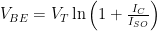
, where IC is the collector current, ISO is the saturation current of the base-emitter diode, and VT is the thermal voltage V_{T} = \frac{k_{B} T}{q} \approx 26 mV at 300º K.  I should be able to estimate VT and ISO from the log amplifier measurements I made earlier. (I get VT =25.6mV and ISO=7.9E-15A for S9013.)

Along the way, I realized that I had never plotted a voltage-versus-current curve for the Schottky diodes, to confirm the theoretical formula V = V_{T} \ln \left ( 1+ \frac{I_{C}}{I_{S}}\right)
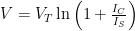
, where IS is the saturation current of the diode.

I did those measurements this morning, using a 1N5817 Schottky diode, a series resistor, a series potentiometer, and an Arduino (Leonardo) board.  I measured the voltage across the resistor (to get current) and across the diode.

The voltage does fit nicely to the log of current, with IS=1.32µA and VT=27.1 mV. Given the quantization noise in the voltage measurement, these seem like a pretty good fit to theory.

The voltage does fit nicely to the log of current, with IS=1.32µA and VT=27.1 mV. Given the quantization noise in the voltage measurement, these seem like a pretty good fit to theory. (click to embiggen)

When my son gets the Data Logger working with the KL25Z boards, I’ll probably want to redo these measurements with higher precision. Note that both VT and IS depend on temperature, and I did not measure the temperature (probably around 18ºC). IS normally doubles for every 10ºC temperature rise, so any measuring device relying on these characteristics would need to have temperature compensation or calibration to correct for temperature.  In any event the IS values for the Schottky diodes are much larger than for the base-emitter junctions, so voltage drop across the diode is much smaller for a given current—which is why we use Schottky diodes!

2013 July 16

Precision rectifier

Filed under: Circuits course,Data acquisition — gasstationwithoutpumps @ 11:36
Tags: , , , , , ,

The log amplifier that I’ve spent the last several days understanding (posts a, b, c) is not the only non-linear circuit needed for a loudness detector.  We also need to convert the audio input signal into a slowly changing amplitude signal that we can take the logarithm of.  As I discussed in the first post on log amps, I had rejected true-RMS converter chips as too expensive for the application (though the original application has gone away), and decided to try a rectifier and low-pass filter.

[Incidentally, my son is now looking at a different processor chip, the KL25 from Freescale (an ARM Cortex chip), which has a 16-bit ADC that is much faster than the ATMega’s, so the entire loudness-detector could be done in software, except for a one-op-amp preamplifier.  With a  16-bit ADC, we can get almost 90dB of range without needing a log amplifier. We’re planning to order a development board that is compatible with Arduino shields (but has lots more I/O pins available) and that has an accelerometer on the board.  Amazingly, the development board is only $13, about half the price of an Arduino.]

A single diode does not work for our rectifier needs in the loudness circuit, because diodes don’t turn on until the voltage across them is at least a “diode drop” (about 0.7v for silicon diodes and 0.45v for Schottky diodes).  However, the simple circuit for the log amplifier is also the circuit for a precision rectifier:

This circuit is both a log amplifier and a precision rectifier.  If Vb is set to a constant voltage, then Vout1-Vb varies as log(Vb-a).  Vout2 is max(Va,Vb).

This circuit is both a log amplifier and a precision rectifier. If Vb is set to a constant voltage, then Vout1 varies as log(Vb–Va). Vout2 is max(Va,Vb). 
The diode can be connected in the opposite direction, to get Vout2=min(Va,Vb) and Vout1 varying with log(Va–Vb).

The log-amplifier circuit I used in the previous posts had a transistor in place of the diode, so that the crucial voltage that was being exponentiated was referenced to the bias voltage, rather than the input. We also needed a compensation capacitor in parallel with the transistor to prevent oscillation in the negative feedback loop.

For the precision rectifier, we swap the inputs, so that Va is the signal input and Vb is a constant threshold voltage for the rectifier. We do not need (or want) the compensation capacitor, as that would cause the circuit to act as a unity gain amplifier at high frequency, rather than as a rectifier.

Because I did not happen to have any diodes, but had plenty of transistors, I experimented with the rectifier circuit using diode-connected bipolar transistors (collector and base connected together). Because the output of the rectifier is not directly driven by an op amp, I used unity-gain buffers to isolate the test circuitry (Arduino analog inputs or BitScope oscilloscope) from the amplifier:

Test circuit for low-speed testing of precision rectifier circuit.

Test circuit for low-speed testing of precision rectifier circuit. Here the NPN transistor is used as a diode, in the opposite direction as in the first schematic, so Vout should be min(Vin, Vbias)

My initial test setup did not have the unity-gain buffer for Vin, but I found that one of my Arduino analog input pins was quite low impedance and was discharging my capacitor. Switching to a different pin helped, but I eventually decided to avoid that kluge and use a unity-gain buffer instead.

I tried several different values for R2. The most predictable effect of changing the value is a change in the range over which the rectifier operates. Clipping occurs because the output of the op amp is limited to be between the rails of the power supply. The feedback transistor is conducting when the rectifier is following the input, so the op amp output has to be substantially lower than Vout.  The function implemented is max(Vclip, min(Va,Vbias)).  Vclip should go down as R2 is increased (at about 60mV for each factor of 10 in resistance—the same shift as in the log amplifier).

Here are a couple of plots of Vout vs. Vin for the S9018 transistor:

With a 1kΩ resistor, the clipping voltage is fairly high, and we have a somewhat limited range for the rectifier.

(click to embiggen) With a 1kΩ resistor, the clipping voltage is fairly high, and we have a somewhat limited range for the rectifier.  The offset voltage for the rectifier between the output and the input is much less than the resolution of the Arduino ADC (about 5mV).

With a 10kΩ resistor, the clipping voltage is lower, giving us more range for the rectifier.

(click to embiggen) With a 10kΩ resistor, the clipping voltage is lower, giving us more range for the rectifier.

Using a PNP transistor instead of an NPN has the effect of reversing the diode and producing Vout=min(Vclip, max(Vin, Vbias)):

With an S9012 PNP transistor and a 10kΩ resistor, we get clipping at the high end.

(click to embiggen) With an S9012 PNP transistor and a 1kΩ resistor, we get clipping at the high end.

With a 10kΩ resistor we get a larger range.

(click to embiggen) With a 10kΩ resistor we get a larger range.

So why not go for a very large resistor and maximize the range? From a DC perspective this looks like a win (though it is hard to see in the limit how Vbias would affect the result if the resistance went to infinity).  Of course, the problem is with high-frequency response.  Consider the difference between the S9018 NPN transistor with a 1kΩ resistor and a 330kΩ resistor:

S9018-330kohm-1kHz

(click to embiggen) With an S9018 NPN transistor and a 330kΩ resistor at 1kHz. Note the overshoot when the rectifier shuts off.

Fairly clean signal with a S9018 NPN transistor and a 10kΩ resistor at 1kHz.

(click to embiggen) Fairly clean signal with a S9018 NPN transistor and a 10kΩ resistor at 1kHz.

With a 1kΩ resistor, there is very little overshoot as the rectifier turns off.

(click to embiggen) With a 1kΩ resistor, there is very little overshoot as the rectifier turns off, but we can see a bit of a problem when the rectifier turns back on.

There is a problem with the rectifier turning on slowly, because Vout has to move all the way from the top rail down to the bias voltage, and the op amp has a slew-rate limitation. This phenomenon can be seen more clearly at a higher frequency:

The S9018 NPN transistor with a 10kΩ resistor and a 15kHz input signal.  The overshoot as the rectifier turns off is about 50mV, and the turn-on delay is about 8µsec.  The turn-on delay does not vary much with the input resistance, unlike the turn-off overshoot.

(click to embiggen) The S9018 NPN transistor with a 10kΩ resistor and a 15kHz input signal. The overshoot as the rectifier turns off is about 50mV, and the turn-on delay is about 8µsec. The turn-on delay does not vary much with the input resistance, unlike the turn-off overshoot.

I believe that the overshoot as the rectifier turns off is due to capacitance, as adding a small feedback capacitor in parallel with the diode increases the overshoot substantially:

With a 33pF capacitor in parallel with the diode (an S9018 NPN transistor), a 10kΩ resistor,  and a 15kHz input, the overshoot goes up to about 290mV from 50mV without the capacitor.

(click to embiggen) With a 33pF capacitor in parallel with the diode (an S9018 NPN transistor), a 10kΩ resistor, and a 15kHz input, the overshoot goes up to about 290mV from 50mV without the capacitor. The turn-on delay is masked somewhat by the high-frequency feedback.

Note: the S9018 has the best high-frequency response (if you consider 15kHZ high frequency) of any of the transistors I looked, probably because it has the lowest capacitance. For example, with a 10kΩ resistor the S9013 NPN has 120mV of overshoot at 15kHz, instead of only 50mV, and the S9012 PNP has -180mV. With a 1kΩ resistor, I can’t measure the overshoot on any of these three transistors. So the limited range with a 1kΩ resistor is compensated for by the much cleaner turn-off behavior.  I should be able to get better range by using a fast-response Schottky diode instead of diode-connected transistor.

Of course, the turn-on behavior is a bigger problem and one that can’t be fixed by playing with the resistor or the diode, because the problem is with the large voltage swing needed from the op amp in order to turn on. There are standard solutions that limit the voltage swing, but I think I’ll leave that for a later blog post.

2013 July 12

Logarithmic amplifier again

Filed under: Circuits course,Data acquisition — gasstationwithoutpumps @ 22:20
Tags: , , , , ,

Yesterday, in Logarithmic amplifier, I ended with the following plot:

The gnuplot fit agrees with the measurements made with the BitScope for 5 resistor values.  The resolution of the Arduino DAC limits the ability to measure the dynamic range.

(click plot to see larger version) The cloud of points is broad enough to be consistent with slightly different parameter values.

I was bothered by the broad cloud of points, and wanted to come up with a better test circuit—one that would give me more confidence in the parameters.  It was also quite difficult to get close to Vbias—the closest this could measure was one least-significant-bit of the DAC away (about 5mV).  A factor of 512 from the largest to the smallest signal is 54dB, but only about the upper 40dB of that was good enough data for fitting (and very little time was spent at near the Vbias value).

I think that part of the problem with the cloud was that the input signal was changing fairly quickly, and the Arduino serializes its ADC, so that the input and output are measured about 120µsec apart.  I decided to use a very simple slow-changing signal: a capacitor charging toward Vbias through a large resistor.  My first attempt used a 1MΩ resistor and a 10µF capacitor, for a 10-second time constant:

Output voltage from log amplifier (with 3x gain in second stage) as capacitor charges. One fit uses the Arduino-measured Vin and Vbias voltages, the other attempts to model the RC charging as well. What are the weird glitches?

Output voltage from log amplifier (with 3x gain in second stage) as capacitor charges. (click picture for larger version) One fit uses the Arduino-measured Vin and Vbias voltages, the other attempts to model the RC charging as well. What are the weird glitches?

The capacitor charging should be a smooth curve exponential decay to Vbias, so the log amplifier output should be a straight line with time. There were two obvious problems with this first data—the output was not a straight line and there were weird glitches about every 15–20 seconds.

The non-straight curve comes from the capacitor not charging to Vbias. Even when the capacitor was given lots of time to charge, it remained stubbornly below the desired voltage. In think that the problem is leakage current: resistance in parallel with the capacitor. The voltage was about 1% lower than expected, which would be equivalent to having a 100MΩ resistor in parallel with the capacitor.  I can well believe that I have sneak paths with that sort of resistance on the breadboard as well as in the capacitor.

According to Cornell Dublier, a capacitor manufacturer, a typical parallel resistance for a 10µF aluminum electrolytic capacitor would be about 10MΩ [http://www.cde.com/catalogs/AEappGUIDE.pdf‎]:

Typical values are on the order of 100/C MΩ with C in μF, e.g. a 100 μF capacitor would have an Rp of about 1 MΩ.

So I may be lucky that I got as close to Vbias as I did.

The glitches had a different explanation: they were not glitches in the log amplifier circuit, but in the 5V power supply being used as a reference for the ADC on the Arduino board—I had forgotten how bad the USB power is coming out of my laptop, though I had certainly observed the 5V supply dropping for a second about every 20 seconds on previous projects.  The drop in the reference for the ADC results in a bogus increase in the measured voltages.  That problem was easy to fix: I plugged in the power supply for the Arduino rather than running off the USB power, so I had a very steady voltage source using the Arduino’s on-board regulator.

    With a proper power supply, I get a clean charge and the output is initially a straight line, but I'm still not getting close to Vbias.  Again the blue fit uses the measured Vin and Vbias voltages, while the green curve tries to fit an RC decay model. Note the digitization noise on the measured inputs towards the end of the charging time.

(click picture for larger version) With a proper power supply, I get a clean charge and the output is initially a straight line, but I’m still not getting close to Vbias. Again the blue fit uses the measured Vin and Vbias voltages, while the green curve tries to fit an RC decay model. Note the digitization noise on the measured inputs towards the end of the charging time.

To solve the problem of the leakage currents, I tried going to a larger capacitor and smaller resistor to get a similar RC time constant. At that point I had not found and read the Cornell Dublier application note, though I suspected that the parallel resistance might scale inversely with the capacitor size, in which case I would be facing the same problem no matter how I chose the R-vs-C tradeoff. Only reducing the RC time constant would work for getting me closer to Vbias.

Using a 47kΩ resistor and a 470µF capacitor worked a bit better, but the time constant was so long that I got impatient:

(click image for larger version) The blue fit is again using the measured Vin and Vbias, and has a pretty good fit.  The green fit using an RC charge model does not seem quite as good a fit.

(click image for larger version) The blue fit is again using the measured Vin and Vbias, and has a pretty good fit. The green fit using an RC charge model does not seem quite as good a fit.

The calibration of 9.7mV/dB seems pretty good, so the 409mV range of the recording corresponds to a 42dB range. The line is straighter, but I’m still not getting as close to Vbias as I’d like.

I then tried a smaller RC time constant (hoping that the larger current with the same capacitor would result in getting closer to Vbias, and so testing a larger dynamic range on the log amplifier). I tried 16kΩ with the 470µF capacitor:

(click image to embiggen) I'm now getting a clear signal from the log amplifier even after the input voltage has gotten less than one least-significant-bit away from Vbias.  I found it difficult to fit parameters for modeling the RC charge.

(click image to embiggen) I’m now getting a clear signal from the log amplifier even after the input voltage has gotten less than one least-significant-bit away from Vbias (the blue fit). I found it difficult to fit parameters for modeling the RC charge (the green fit).

The two models I fit to the data give me somewhat different mV/dB scales, though both fit the data fairly well. The blue curve fits better up to about 65 seconds, then has quantization problems. Using that estimate of 9.8mV/dB and the 560mV range of the output, we have a dynamic range here of 57dB. There is still some flattening of the curve—we aren’t quite getting to the Vbias value, but it is pretty straight for the first 50 seconds.

Note: the parallel resistance of the capacitors would not explain the not-quite-exponential behavior we saw in the RC time constant lab, since those measurements were discharging the capacitor to zero. A parallel resistance would just change the time constant, not the final voltage.

I was using the Duemilanove board for the log-amplifier tests. I retried with the Uno board, to see if differences in the ADC linearity make a difference in the fit:

    Using the Uno Arduino board I still had trouble with the fit, and the Uno ADC seems to be noisier than the Duemilanove ADC.  The missing parts of the blue curve are where the Uno board read the input as having passed Vbias.

(click to embiggen) Using the Uno Arduino board I still had trouble with the fit, and the Uno ADC seems to be noisier than the Duemilanove ADC. The missing parts of the blue curve are where the Uno board read the input as having passed Vbias.

The 625 mV range over 250 seconds corresponds to about 69dB, assuming that the 9.1 mV/dB calibration is reasonably accurate (and 64dB if the earlier 9.8mV/dB calibration is better).
My measurements of the log amplifier do not seem to yield a very consistent mV/dB parameter, with values from 9.1mV/dB to 9.8mV/dB using just the Arduino measurements (and even less consistency when a model of RC charging is used).  I’m not sure how I can do more consistent measurements with the equipment I have.  Anyone have any ideas?
Incidentally, my son has decided not to include a microphone in his project.  The silicon MEMS mic was small enough, but the op amp chip for the analog processing was too big for the small board area he had left in his layout, and he decided that the loudness detector was not valuable enough for the board area and parts cost. I believe that his available board area shrunk a little today, because he discovered that the keep-away check had not been turned on in the Eagle design-rule checker.  Turning it on indicated that he had packed the capacitors too close in places, and he had to spread them out. (At least, I think that’s what he told me—I’ve not been following his PC board layout very closely.)
I’m still interested in learning about log amplifiers and precision rectifiers, so I’m still going to breadboard the components of the design and test them out.  I’m not sure when I’ll ever use the knowledge, since the Applied Circuits course does not cover the nonlinear behavior of pn junctions nor the forward-voltage drop of diodes (we don’t use diodes in the course).

2013 July 11

Logarithmic amplifier

Filed under: Data acquisition — gasstationwithoutpumps @ 23:16
Tags: , , , , ,

My son wanted to design a circuit to convert microphone inputs to loudness measurements usable by an Arduino (or other ATMega processor).  We discussed the idea together, coming up with a few different ideas.

The simplest approach would be to amplify the microphone then do everything digitally on the Arduino. There are several features of this approach:

  • The analog circuit is about as simple as we can get: a DC-blocking capacitor and an amplifier.  This would only need one op amp, one capacitor, and 2 resistors (plus something to generate a bias voltage—perhaps another op amp, perhaps a low-drop-out regulator).
  • Using digital processing, he can do true RMS voltage computation, and whatever low-pass filtering to smooth the result that he wants.
  • He can’t sample very fast on the ATMega processor, so high frequencies would not be handled properly.  He might be able to sample at 9kHz (about as fast as the ADC operates), but that limits him to 4.5kHz. For his application, that might be good enough, so this doesn’t kill the idea.
  • He’d like to have a 60dB dynamic range (say from 50dB to 110dB) or more, but the ADC in the ATMega is only a 10-bit converter, so a 60dB range would require the smallest signal to be ±½LSB, which is at the level of the quantization noise.  With careful setting of the gain for the microphone preamp, one might be able to get 55dB dynamic range, but that is pushing it a bit.  The resolution would be very good at maximum amplitude, but very poor for quiet inputs.

Although the mostly digital solution has not been completely ruled out, he wanted to know what was possible with analog circuits.  We looked at two main choices:

  • True-RMS converter chips (intended for multimeters).  These do all the analog magic to convert an AC signal to a DC signal with the same RMS voltage.  Unfortunately, they are expensive (over $5 in 100s) and need at least a 5v power supply (he is planning to use all 3.3v devices in his design).  Also true RMS is a bit of overkill for his design, as log(amplitude) would be good enough.
  • Using op amps and discrete components to make an amplifier whose output is the logarithm of the amplitude of the input.  Together we came up with the following block diagram:
Block diagram of the loudness circuit.

Block diagram of the loudness circuit. (drawn with SchemeIt).

We then spent some time reading on the web how to make good rectifier circuits and logarithmic amplifiers. I’ll do a post later about the rectifier circuits, since there are many variants, but I was most interested in the logarithmic amplifier circuits, which rely on the exponential relationship between current and voltage on a pn junction—often the emitter-base junction of a bipolar transistor.

My son wanted to know what the output range of the log amplifier would be and whether he would need another stage of amplification after the log amplifier. Unfortunately, the theory of the log amplifier uses the Shockley ideal diode equation, which needs the saturation current of the pn junction—not something that is reported for transistors.  There is also a “non-ideality” parameter, that can only be set empirically.  So we couldn’t compute what the output range would be for a log amplifier.

Today I decided to build a log amplifier and see if I could measure the output.  I also wanted to figure out what sort of dynamic range he could get from a log amp. Here is the circuit I ended up with, after some tweaking of parameters:

The top circuit is just a bias voltage generator to create a reference voltage from a single supply. I'm working off of 5v USB power, so I set the reference to 2.5v. He might want to use a 1.65v reference, if he is using 3.3v power. The bottom circuit is the log amplifier itself.

The top circuit is just a bias voltage generator to create a reference voltage from a single supply. I’m working off of 5v USB power, so I set the reference to 2.5v. He might want to use a 1.65v reference, if he is using 3.3v power.
The bottom circuit is the log amplifier itself.

I chose a PNP transistor so that Vout would be more positive as the input current got further from Vbias.  I have 6 different PNP transistors from the Iteadstudio assortment of 11 different transistors, and I chose the A1015 rather arbitrarily, because it had the lowest current gain. I should probably try each of the other PNP transistors in this circuit, to see how sensitive the circuit is to the transistor characteristics.  I suspect it is very sensitive to them.

The circuit only works if the collector-base junction is reverse-biased (the usual case for bipolar transistors), so that the collector current is determined by the base current. The emitter-base junction may be either forward or reverse biased.  Note that if Vin is larger than Vbias, the collector-base junction becomes forward-biased, the negative input of the op amp is slightly above Vbias, and the op amp output hits the bottom rail.

As long as Vin stays below Vbias, the current through R2 should be \frac{V_{bias} - V_{in}}{R_{2}}
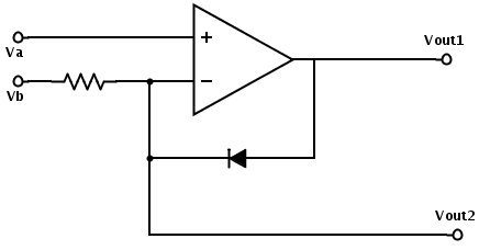
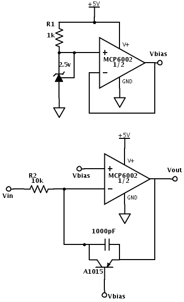
, and the output voltage should be V_{out}-V_{bias} = A \ln \frac{B(V_{bias} - V_{in})}{R_{2}} for some constants A and B that depend on the transistor. Note that changing R2 just changes the offset of the output, not the scaling, so the range of the output is not adjustable without a subsequent amplifier.

The 1000pF capacitor across the transistor was not part of the designs I saw on the web, but I needed to add it to suppress high-frequency (around 3MHz) oscillations that occurred. The oscillations were strongest when the current through R2 was large, and the log output high.  I first tried adding a base-emitter capacitor, which eliminated the oscillations, but I still has some lower-frequency oscillations when the transistor was shutting off (very low currents).  Moving the capacitor to be across the whole transistor as shown in the schematic cleaned up both problems.

I put ramp and sine wave inputs into the log amplifier.  The waveforms were generated with the Bitscope function generator, which does not allow setting the offset very precisely—there is only an 8-bit DAC generating the waveform.  Here is a sample waveform:

The green trace is the input, the yellow trace is the output.  The horizontal axis in the middle is at 2.5V for the input (so the input is always below 2.5V) and at 3V for the output.  THe scale is 1V/division for the input and 50mV/division for the output.

Click picture for larger image. The green trace is the input, the yellow trace is the output. The horizontal axis in the middle is at 2.5V for the input (so the input is always below 2.5V) and at 3V for the output. The scale is 1V/division for the input and 50mV/division for the output.  [And all those values should be visible in the saved snapshot, but they aren’t.]

The ripple on the output is mainly artifacts of the low-resolution of the BitScope A-to-D converter—smoothing of multiple reads is done, but there is a lot of quantization noise. According to my analog scope there are still some 24MHz noise around, but it seems to be from the Vbias source—adding a 4.7µF capacitor between Vbias and +5V (adjacent pins on the op amp) cleaned things up a lot on the analog scope, without affecting the BitScope traces.

Using the cursors on the BitScope, I was able to measure the output voltages for input voltages of Vbias-0.5V, Vbias-1V, and Vbias-2.5V.  From these, I concluded that the scaling factor for the output was about 3.1–3.2 mv/dB.  The output was 3±0.07V, so the dynamic range is 140mV/(3.2 mv/dB), or about 44dB.  We can see the logarithmic response in an X-Y plot of the output vs the input:

Output vs. input of the log amplifier.  Note that the output is the log of Vbias-Vin, so the log curve looks backwards here.

(Click for larger image) Output vs. input of the log amplifier. Note that the output is the log of Vbias-Vin, so the log curve looks backwards here.  It’s a shame that BitScope throws away the grid on XY plots, as the axes are still meaningful.

I also tried using an external oscillator, so that I could get better control of the offset voltage, and thus (perhaps) a better view of the dynamic range. I could fairly reliably get an output range of about 200mV, without the hysteresis that occurs when the collector-base junction gets forward biased. That would be over 60dB of dynamic range, which should be fine.

I should be able to adjust the voltage offset of the amplifier by changing R2. Increasing R2 reduces the current, which should lower the voltage. I tried several different values for R2 and measured the maximum output voltage, using the same input throughout:

1kΩ 3.106v
10kΩ 3.056v
100kΩ 2.992v
1MΩ 2.936v

The 60dB difference in current produces a 170mV difference in output, for 2.83 mV/dB.

Oops, those weren’t quite all the same, as the load from the resistor changes the input. Adding a unity-gain buffer driving the inputs and adjusting the input so that the output of the unity gain buffer has a slight flat spot at 0V gives me a new table:

1kΩ 3.12v
10kΩ 3.06v
100kΩ 3.00v
1MΩ 2.94v
5.6MΩ 2.90v

which is consistent with 3mV/dB. I was not able to extend this to lower resistances, as I started seeing limitations on the output current of the op amp. But it is clear that the amplifier can handle a 75dB range of current, with pretty good log response.

An Arduino input is about 5mV/count, so the resolution feeding the output of the log amplifier directly into the Arduino would be about 1.7dB/count. We could use a gain of 4 without saturating an op amp (assuming that we use 2.5V as the center voltage still), for about a 0.4 dB resolution. More reasonably, we could use a gain of 3 to get a resolution of about 0.54dB/count.

I tried that, getting the following table:

1kΩ 4.46v
10kΩ 4.28v
100kΩ 4.10v
1MΩ 3.91v
5.6MΩ 3.78v

This table is consistent with 9.1 mv/dB, for a resolution of about 0.54 dB/step on the Arduino.

I tried using the Arduino to collect the same data and fit with gnuplot:

The gnuplot fit agrees with the measurements made with the BitScope for 5 resistor values.  The resolution of the Arduino DAC limits the ability to measure the dynamic range.

(click plot to see larger version) The gnuplot fit agrees fairly well with the measurements made with the BitScope for 5 resistor values. The resolution of the Arduino DAC limits the ability to measure the dynamic range, and the cloud of points is broad enough to be consistent with slightly different parameter values.

The next thing for me to do on the log amp is probably to try different PNP transistors, to see how that changes the characteristics. My son will probably want to use a surface-mount transistor, so we’ll have to find one that is also available as a through-hole part, so that we can check the log amplifier calibration.