Gas station without pumps

2021 June 21

Controlling current

Filed under: Circuits course — gasstationwithoutpumps @ 11:06
Tags: , , ,

In the electrode lab this year, students had even more trouble than usual in understanding that the the goal was to provide a constant current to the silver-wire electrodes for a measured time period, in order to produce a known amount of AgCl on the anode.  I will have to rewrite that section of the book for greater clarity.  I also plan to add a circuit that does the constant-current control for them, so that they don’t have to adjust the voltage to get the desired current (a concept that seems to have eluded many of them).

Here is a possible circuit:

Current-control-for-low-current

This circuit provides a current from Ip to Im of Vri/Rsense, as long as the voltage and current limitations of the op amp are not exceeded.

The negative-feedback loop tries to bring the I_m output to the voltage of the V_{\rm ri} input, which is only possible if the current through the sense resistor is I=V_{\rm ri}/R_{\rm sense}.  Let’s say that we want 1mA from Ip to Im—then we would set V_{\rm ri}= (1\,mA) R_{\rm sense} = (1\,mA)(100\Omega) = 100\,mV.  If V_{\rm rail} is 5V and the op amp is a rail-to-rail op amp, then we could get the desired 1ma of output as long as the load resistance from Ip to Im is less than 4900Ω (well, 4650Ω really, because of the internal resistance of the op amp).  With a higher load resistance, the voltage at Ip would hit the top rail and still not provide the desired current.  There is no lower limit to the load resistance—even with a short circuit the current would be the desired 1mA.

I chose 100Ω for the sense resistor, so that the control voltages do not get too close to the bottom rail, while leaving enough voltage range for fairly large load resistances.  By using 100Ω, it is possible to specify currents up to 50mA, which is beyond the capability of the op amp to supply.  Since the MCP6004 op amps have a short-circuit current of about 20mA with a 5V supply, about the most we can deliver is 14mA for a short-circuit load, because of the internal resistance of the op amp.  

Using a 1kΩ resistor might also be reasonable, since the input voltage in volts would then specify the current in mA, but a 1mA output current would limit the voltage across the output ports to V_{\rm rail} -1\,V (which is probably still fine for the electrode lab). With a 1kΩ resistor and a 5V supply, the maximum specifiable current would be 5mA, and the maximum obtainable is about 4mA.  If you needed 2V across the load, then you could not specify more than 2.4mA (still plenty for the electrode lab).

For the electrode lab, the currents required are low enough that this circuit is adequate, but what if we needed more current?  Here are a couple of circuits that can provide that:

Current-control-with-pFET

By using a pFET, we can have the voltage output of the op amp control the current. No current is needed from the op amp, and we just need that Vrail is large enough that the pFET can be fully turned on.


Current-control-with-PNP

If we use a PNP transistor, then we need to turn the voltage output of the op amp into a current for the base.  That current is about 1/50th or 1/100th of the collector current being controlled (depending on the transistor).

Both these designs have the positive and negative inputs of the op amp reversed from the low-current design, because the pFET or PNP transistor provides a negation—the voltage at Im rises as the voltage at the output of the op amp falls.  I reduced to the sense resistor to 10Ω, to allow specifying higher currents (up to 500mA for a 5V supply).  The main limitations on this design are the thermal limitations of the transistor and the resistor—there may be both a large voltage drop and a large current.  The worst case for the transistor is when the load is a short circuit and the voltage at Im is half the power-supply voltage—then the power dissipated in the transistor (and in the sense resistor) is (V_{\rm rail}/2)^2/10\Omega.  For a 400mW limitation on the transistor, we would want to limit V_{\rm rail} to 4V.  For a ¼W resistor, we would want to limit V_{\rm ri} to 1.58V (specifying 158mA), or up the resistor to 100Ω for a 5V limit (but then we could only specify up to 50mA).  We really need a 2.5W resistor if we want to have 10Ω and a 5V supply and use the full range.

For the book, I think I’ll just present the low-current version of the current control—we don’t need the high-current version, and students are likely to request too much current for the electroplating if they have it available (errors in computing the area of the electrodes that are off by a factor of 100 are pretty common—mixing up ({\rm mm})^2 and ({\rm cm})^2, for example).

2020 March 26

Screaming op amp

Filed under: Circuits course — gasstationwithoutpumps @ 20:12
Tags: , ,

Santa Cruz’s Museum of Art and History is having a “drawing activity” online while the museum is closed, based on their 2017 Screaming Hand Exhibit.

I’d like to see a screaming banana slug, but I can’t draw, so I  created a screaming op amp for the students in my electronics course:

I think that this circuit accurately reflects how many of the students in my class feel.

I used Digi-Key’s SchemeIt for the schematic and edited the mouth using Gimp and Inkscape from a low-quality image of a screaming-hand sticker (possibly not legally licensed) that I found with Google image search.  MAH provides a PDF file for you to start with, assuming that you will draw and color around the  printed mouth, but I find cutting and pasting SVG files in Inkscape easier.

I now have an SVG file of the screaming op amp, which I could scale up to T-shirt size, if needed.

2019 August 21

Gain-bandwidth product

Filed under: Circuits course — gasstationwithoutpumps @ 17:15
Tags: , ,

I spent yesterday afternoon collecting data for two figures for my book illustrating the limitation on gain caused by the gain-bandwidth product:

This graph shows the measured gain of non-inverting amplifiers built using the MCP6004 op amp.
It also includes a line for f_{GB}/f fit to the data for the highest-gain amplifier.

This graph compares the measured data (thin lines) to the model used in the book for amplifiers with gain-bandwidth limitations (thick yellow lines) for three of the amplifier configurations.

I did all the data collection with my Analog Discovery 2, using the network analyzer.

The data looks easy to collect, and I expected it to take me just an hour to gather all the data, but it was a bit trickier than I thought. I used a symmetric ±2.5V power supply from the Analog Discovery 2, so all the signals could be centered at 0V.

One problem was that I initially had not set the offset and gain of the oscilloscope channels to “auto”, and the output was not centered precisely at 0V. The network analyzer does not do as good a job of compensating for DC offsets as I think it should. I set the channels to automatic gain and offset and I tweaked the offset of the waveform generator by 1mV to make the output be centered correctly. I think that the 1mV offset is compensating for the offset of the op-amp chip, but it may be correcting an offset in the waveform generator.

For the high-gain amplifiers, I needed to reduce the signal from waveform generator, because the smallest signal the network analyzer allows is ±10mV, and with a gain of 393, that would cause clipping. My first voltage divider reduced the signal sufficiently, but I got very noisy results. It took me quite a while to realize that the problem was not just loose wires (though those were also a problem), but that I had used resistors that were too large, so that the input of the amplifier was amplifying capacitively coupled 60Hz noise. Reducing the input voltage divider to 1kΩ resistors solved that problem.

I was having another problem in which the shape of the curve for the low-gain amplifiers changed at the high-frequency end as I changed the amplitude of the signal. It took me an embarrassingly long time to realize that the problem was that I was hitting slew-rate limits before hitting the gain-bandwidth product limits. The high-gain amplifiers all had much lower gain at 1MHz than at low frequencies, so an input signal small enough to avoid clipping at low frequencies produced such a small output at high frequencies that slew rate was not limiting. But for low-gain amplifiers, I had been increasing the amplitude for better measurements, and the gain at 1MHz was only a little less than the gain in the passband, so I was asking for over 8V/µs, and the amplifier’s slew rate is only 0.6V/µs. I realized the problem when I used the oscilloscope to look at what the amplifier was producing, and saw that it was not a sine wave, but a small weirdly distorted signal.

After I finally got everything set up and working with small enough inputs to avoid clipping in high-gain amplifiers and slew-rate limitations in low-gain amplifiers, I finally was able to collect a consistent set of data.

The model for the op amp is that the open gain is A =  \frac{1}{1/A_0+ jf/f_{GB}} \approx  -j f_{GB}/f
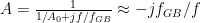
, and the gain of the non-inverting amplifier is \frac{A}{1+AB} \approx  \frac{1}{B}\; \frac{1}{1+jf/(B f_{GB})}, where B is just the gain of the voltage divider used as a feedback network. The model breaks down at high frequencies, because the op amp has further filtering above 1MHz, and for very high gain, where the DC amplification limit A_0 matters. We don’t design op-amp circuits to use such a high gain that the DC open-loop gain matters, but pushing the frequency limit is common.

But the simple gain-bandwidth model does a very good job of fitting the data, as long as you avoid signal levels that cause clipping or slew-rate limitations.

2015 July 8

Testing nFET body diode with function generator

Filed under: Circuits course — gasstationwithoutpumps @ 23:54
Tags: , , , ,

Continuing yesterday’s post on the i-vs-v characteristics of the PSMN022-30PL nFETs, I decided to look at the body diode characteristics. I changed the circuit only slightly from

Circuit for measuring I-vs-V characterisitics of nFET.

Circuit for measuring I-vs-V characteristics of nFET.

to

The circuit is essentially the same, but some of the wires are swapped to make measurements all be in 0–3.3V range.

The circuit is essentially the same, but some of the wires are swapped to make measurements all be in 0–3.3V range.

The plots I got were the exponential dependence of current on voltage that I expected:

The leakage current around 6nA may be from the breadboard or ADC—note that the load resistor here is an open circuit, getting about 170MΩ resistance from the breadboard or the KL25Z ADC inputs.

The leakage current around 6nA may be from the breadboard or ADC—note that the load resistor here is an open circuit, getting about 170MΩ resistance from the breadboard or the KL25Z ADC inputs.

To get the straight lines to fit so nicely, I had to do two things: throw away any points where E20  was less than 5mV or E21 was greater than 3.29V (the voltages may have been going outside the ADC range of 0V–3.3V, and the last few counts at each and of the range are always a bit suspect), and subtract a tiny offset from the E20 voltage (1.2mV).

I did run into one surprising phenomenon: the max current was not as high as I expected.  With a 47Ω output impedance from the FG085 and a 10V maximum voltage, I expected the 27Ω resistance to give me a current of about (10V - 0.7V)/ (27\Omega + 47\Omega) = 126mA, but I only got 77mA.  I investigated further and looked at the voltage across a 27Ω resistor with no FET:

Both currents are show as positive, for convenience in plotting (as the KL25Z only records positive voltages—I swapped leads on the function generator to examine negative swing.

Both currents are show as positive, for convenience in plotting (as the KL25Z only records positive voltages—I swapped leads on the function generator to examine negative swing.

The triangle waves, which look ok with no load or with large impedance loads, get very distorted at high currents.  For triangle waves going positive, the current starts getting limited at about 72mA, and strong clipping kicks in at about 80mA.  For triangle waves going negative, the current starts getting limited at 50mA, and strong clipping kicks in around 65mA.  The clipping actually gets stronger as the voltage of the source attempts to rise further, so the waveform isn’t flat on top but dips.

Unfortunately, the current limits do not seem to be a simple thing.  Using a 3Ω load instead of a 27Ω load gets different values for the limits:

With a 3Ω load, the ultimate current limits are substantially higher.

With a 3Ω load, the ultimate current limits are substantially higher.

For positive wave forms, the limitation starts at around 74mA with strong clipping at 93mA, and for negative transitions limitations start around 52mA with strong clipping at 80mA. The values where the current limiting starts are about the same as before, but the strong clipping limits have gone way up.   It is probably reasonable to treat the FG085 as really having  either ±50mA current limits or –50mA,+72mA limits.  The specs for the LM6172 op-amp that drives the output is typical ±60mA, min ±50mA, so treating the limits as ±50mA seems reasonable.

Note that the bad glitches from the cheap fake DAC used in the FG085 are very evident in these plots—the glitches are at each of the high-order bit transitions, with the really big glitch in the middle of the output range (switching from 0x7F to 0x80).  The glitch there is about 3.2LSB (that is, the voltage for 0x80 is slightly less than for 0x7D), which is really terrible for an 8-bit DAC. The 0x40 transition has about a 1.5LSB glitch, and the 0x20 transition about a 0.7LSB glitch. Using a cheap DAC0800 multiplying DAC would have added about 50¢ to their parts and assembly cost (a big deal for a $50 retail product), but allowed them to increase the sampling rate and avoided the non-linearities.  Switching to a better microprocessor (like the KL25 from Freescale could have gotten them more bits, better linearity, and a fast sampling rate at no higher parts cost than the ancient ATMega processor they chose).

I noticed one other problem with the FG085 function generator when doing these measurements—the buttons have very weak springs and often don’t return after being pressed, because the caps rub against the holes in the panel (they made the holes a bit too small or used buttons with crummy springs).  If the button stays down, subsequent button presses look to the firmware like the earlier button pressed again.  I often had to flick the button back up by pressing it up from below the panel—not an ideal user interface!

2015 May 8

First instrumentation-amp lecture

I started today’s lecture by returning a parts-and-tools kit to a student who had left it in lab yesterday—but admonished students not to tease him, since I had left my laptop in the classroom on Wednesday (a much more valuable item in a much less secure location).  That’s the second time in about a year that I’ve left my laptop in a classroom, which is something I never used to do.  (Of course, I’ve been using my laptop in classes a lot more than I used to, so it may not be that I’m getting old and forgetful, just that I have had more opportunities to leave it behind.)

I talked to the students about color-coding their wiring on their breadboards and on their prototyping boards.  The main lesson about color-coding was that black was reserved for ground, red for the positive power supply, and that I had four other colors available for them (blue, green, yellow, and white) in 22-gauge wire. They also have 24-gauge wire in the lab in white and orange, but I’m trying to discourage the use of 24-gauge wire, since it is not well held by the breadboards or KL25Z-board headers, and debugging the loose wires is a pain. I told them that I would not help them debug any boards that did not follow the red and black convention (red for all connections to the positive power supply and for nothing else, black for all the ground wires and nothing else). The other wires I suggested be color-coded on both the schematic and the board, based on the function. For example, all the virtual-ground wires might be white, all the input wires blue, all the wires after pre-amplification green, and so forth.  The exact color coding they use doesn’t matter, as long as they document it clearly and use it consistently.

Hmm, it looks like I’ve never blogged about the newer version of the prototyping boards, so I should include a picture here. I did include a picture before in Twenty-first day of circuits class:

Instrumentation amplifier protoboard with circuit wired for the pressure sensor lab (top left connector to pressure sensor, bottom center connect or to Arduino)

Instrumentation amplifier protoboard with circuit wired for the pressure sensor lab (top left connector to pressure sensor, bottom center connect or to Arduino)

Here is a layout as represented in the Eagle program. Most of the PC board wiring is on the bottom layer, but the +5V power supply crosses over on the top layer (the red trace).  We’ll actually use the 3.3V supply on the KL25Z boards, not +5V power, but that is a minor detail.

This is a layout of the board as shown by Eagle.

This is a layout of the board as shown by Eagle.

The students are given a worksheet for them to plan their layouts on:

This layout worksheet is distributed to the class as a PDF file.  The students can either mark up the PDF with  PDF editing tools (which some students have done successfully in the past), or draw on it with pencils or colored pencils. Only the holes that wires can be placed in are shown—the holes intended for components are omitted from this worksheet.

This layout worksheet is distributed to the class as a PDF file. The students can either mark up the PDF with PDF editing tools (which some students have done successfully in the past), or draw on it with pencils or colored pencils.
Only the holes that wires can be placed in are shown—the holes intended for components are omitted from this worksheet.

I also talked about the importance of keeping wires short and close to the board, and of not routing wires over components.  I’m not expecting students to really internalize that message until they’ve had to debug an inaccessible chip in a nest of long wires, but I’ll put the message out there as often as I can.  I’ve already grumbled at several students in lab for having incomprehensible tangles of wires that were all one color, and I’ll continue to do so.

After the brief warm-up on wire colors, I talked about instrumentation amps as circuit blocks—how they differed from op amps, though both look like differential amplifiers. The key is that op amps have unspecified gain and offset, so need to be used in a negative feedback circuit, which turns them in to amplifiers for single-ended inputs, with inputs and outputs both referenced to a single Vref.  The instrumentation amp has a specified gain (usually controlled by a single external resistor) and a true differential input, with the output still referenced to an external Vref input.

I talked about the output voltage limits of the INA126PA chips they’ll be using, but I did not go to the data sheet to look up the limits, but made up some approximate ones.  I warned them that I was making up approximate ones and that they needed to look the real limits up on the data sheet, but I’m betting that over half the class won’t do that, preferring to believe numbers in their notes that they have been told are fake to looking up the real numbers.

I then had the students help me create a Vref source (a pair of resistors in a voltage divider, followed by a unity-gain buffer), so that we could take current from Vref without violating the voltage-divider constraint.

I showed the students the prototyping board worksheet and where all the components went, and explained how to use the worksheet to do layout before soldering.

I ran out of time, so on Monday, I’ll have to talk about the pressure sensors they’ll be using, and about what the inside of an instrumentation amp consists of (how to build one out of op amps).  I’ll want to do both the 3-op-amp design and the 2-op-amp design, because I’m going to have them build their EKGs in the last week using the 2-op-amp design.

Next Page »