After a discussion in the comments of Ron vs Vgs for pFETs and nFETS with Michael Johnson, I decided to design my own breakout boards for SOT-23 surface-mount FETs, with the possible use of them in the class-D amplifier lab in place of the through-hole TO-220 FETs we’ve been using.
I picked a couple of 30V FETs (one nFET, one pFET) whose data sheets indicated that they would have adequately low on-resistance with a gate voltage of only 2.5V (–2.5V for the pFET), so that the FETs could be controlled by a 3.3V logic signal with no problems. I ended up picking PMV20XNER for nFET (14.9¢ in 100s) and SSM3J332R for pFET (12.4¢ in 100s).
Although the drain-to-source voltage is allowed to go to 30V, the gate-to-source voltage is more limited (±12V for both the nFET and the pFET). That should be adequate for anything we do in the course, as our maximum power supply is ±5V, so we shouldn’t see any voltage differences bigger than 10V. (I could have saved a few cents by using 20V FETs instead of 30V ones, maybe.)
Because the students use the FETs in an H-bridge, I decided to make my breakout board be a half H-bridge, with an nFET, a pFET, a bypass capacitor, and 5 right-angle header pins:

The schematic is quite simple. (The diodes are the body diodes of the FETs.)
The layout took me a while, because I wanted to make as much heat sinking as I could get on a small, cheap board. The standard footprint for a ST-23 allows a thermal resistance of about 120 K/W. I did not push too hard though, because even with ideal layout, the SOT-23 packages still have terrible thermal conductivity (about 90 K/W)—essentially all the heat is being conducted through the thin drain pin. (The SSM3J332R reports even worse numbers: 300 K/W with minimum footprint and 120 K/W with a square inch of copper.)

Solder side of the board. Visualization provided by https://gerber-viewer.easyeda.com/
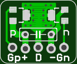
Component side of the board. Visualization provided by https://gerber-viewer.easyeda.com/
My board is not nearly a square inch of copper—the entire board is only 15mm × 12.5mm, and only half of that is used for heatsinking the drains. I used the back of the board for radiating heat and provided thermal vias around the drain pads to connect the front and back. The footprint for the pads is one provided by the manufacturers for wave soldering—I thought it would be easier for had soldering than the much smaller pads used for reflow soldering.
The gate connections are on the outside, the source connections just inboard of them, and the shared drain in the middle. The board is basically symmetric with respect to nFET and pFET, but I labeled the two sides so that there would be less variation in how students soldered them up.
The bypass capacitor is close to the FETs (much closer than the students ever got on a bread board), so we should see less noise injection back into the power rails than we’ve seen in the past. The resistance of the source and drain traces adds another 5mΩ of resistance to the H-bridge, which is not too bad—the beardboard probably adds more like 50mΩ.
If I understood their website correctly, I should be able to get 10 copies of the tiny board panelized in a 6×7 array (so 420 boards after I cut them apart) for only $4.90 from Smart-Prototyping.com. Of course, I’m in a hurry, so I ended up paying an extra $23.79 for shipping with DHL, so the order costs $28.69, or <7¢ a board. I also ordered 10 40-pin right-angle male headers (enough for 80 boards) for $4.11 from AliExpress, raising the price to 12¢ a board.
With the transistors, each half H-bridge will cost under 40¢ in 100s—much less than the approximately $1.37/half H-bridge that the separate TO-220 FETs cost.
The difference in cost is not important for the course ($2 a student), so my main consideration is whether the students will learn more by doing some surface mount soldering with a fixed cMOS half-H-bridge design or by continuing to wire up separate transistors on the bread board (making the usual student errors of getting the pinout wrong or general miswiring). There is still plenty of room for error on the half H-bridge: swapping transistors, getting 2 nFET or 2 pFET instead of one of each, putting the whole board in backwards to short the power supply through the body diodes, …. .
The SOT-23s can’t dissipate quite as much heat as the TO-220s, but we’ll probably not have much heat to dissipate in reasonable designs. With a 5V supply, 8Ω load, and 73mΩ on-resistance, the power dissipation in the pFET should be only about 28mW and the nFET even less—way less than the 500mW or so that I expect the boards to be able to handle. Shoot-through current is mainly what the students will need to worry about, as that can get quite high with the low on-resistances of both the nFET and the pFET.
I’ve ordered the boards and parts to test out using the SOT-23 FETs and half-H-bridge boards. If they work out well, I’ll probably rewrite the class-D lab to have students do a little surface-mount soldering (SOT-23s are about the simplest intro).

")
 or hardback ($198)")

