Gas station without pumps

2018 April 4

Quiz disappointment

Filed under: Circuits course — gasstationwithoutpumps @ 22:31
Tags: , ,

Today’s quiz in class was very disappointing for me, and I don’t know what to do differently to get better results.

Yesterday in lab I returned the quizzes from before break and urged students to look through all the old quizzes and rework any questions they got wrong, reminding them that I recycle questions.

In this morning’s class, before the quiz students asked me to show them (again) how to do one of the questions on the last quiz:

Design a voltage divider implementing Vout − Vref = G(Vin − Vref ), where G can be adjusted from ≈ 0.33 to ≈ 0.67 using a 10 kΩ potentiometer. Use port symbols to connect to Vin, Vref , and Vout.

I showed them two solutions—one that I had expected and a correct, but different solution that a student had come up with.

Here are the two solutions: mine on the left and an alternative one on the right.  (There is a third solution, similar to the second one, but with the potentiometer as variable resistor on the lower leg, rather than the upper one, and the two fixed resistors swapped.)

I had already shown them my solution a week and a half ago, right after they took the quiz, and I had posted both solutions on Piazza.  I not only showed the solution, but gave them an explanation of how it worked again and answered some questions students had about it (like why the gain was expressed the way it was with Vref, and why it was even considered a gain).

Right after that I erased the board and handed out the quizzes.  One of the quiz questions was the identical question that I had just worked on the board for them.  I was resigned to this being a free point for them (just like putting their section number on the quiz is a free point, which I use to distinguish those who are absent from those who are present but get no questions right).

But 20 of the students got no points for the question and 15 got only half credit (out of a class of about 72—there were supposed to be 79, but there were 7 students absent).  So almost half the class could not retain for 5 minutes a simple circuit that they should have been able to derive in a couple of minutes and which they had seen at least 3 times already.

Help!  During the last 10 weeks I’ve gone through just about all the ways I can think of to have the students understand voltage dividers and potentiometers, and I’m obviously not getting through to 28% of them (probably more, since the absentees are likely to be in the group that can’t do the problem also).

Does anyone have any useful advice?  (Giving up on the students is not useful advice—I want them to succeed.)

2016 August 2

The real reason my nFET measurements were bad

Filed under: Circuits course — gasstationwithoutpumps @ 22:54
Tags: , , , ,

In Why my nFET measurements were bad I observed a fixed minimum drain-to-source voltage for my nFET measurements, and claimed that this was the reason I couldn’t get consistent results for the on-resistance of  nFETs when measuring with small currents.

I worried about the result, though, because I really saw no reason for there to be a 20mV minimum Vds voltage. So I did what I should have done right away—set up a negative control. I used a piece of wire to connect the source and drain of the transistor being measured, and did the same Id vs Vds measurements.  This should produce a simple resistance that is very small (a few mΩ for the resistance of the breadboard). But I got the same 20mV minimum voltage as with the nFETs!

The problem turned out to be in my compensation for the offset of the unity-gain buffers—it corrected the value well, but could not correct the range—the smallest ADC output is 0, so if the offset correction makes a 0 ADC value correspond to a positive voltage, then that voltage is the lowest that can be reported.

Today I decided to correct the range as well, by making sure that the op-amp inputs stayed away from 0.  I added 470kΩ pullup to 3.3V to the voltage divider, so that with the input at 0v the output would be at about 83mV.  The Thévenin equivalent of the 470kΩ and 15kΩ resistors is a 14.54kΩ resistor to 102mV.

The new test fixture adds the 470kΩ pullups just to the Vds and Vdd measurements, as Vgs doesn't need to be measured near 0. Noise-reducing capacitors were added to all the op-amp outputs.

The new test fixture adds the 470kΩ pullups just to the Vds and Vdd measurements, as Vgs doesn’t need to be measured near 0.
Noise-reducing capacitors were added to all the op-amp outputs.

I recalibrated the test fixture to get the dividers’ ratios and offsets and measured the nFET again. I tried to let the transistor and load resistor warm up for a while before starting recording for each gate voltage, to avoid thermal drift (there still seems to be some drift for the Vgs=2.89V trace).

Now the curves look much more like the straight lines I expected (and I remembered to test the control: a drain-source short). With lower gate voltages, the nFET could not sink the full current.

Now the curves look much more like the straight lines I expected (and I remembered to test the control: a drain-source short).
With lower gate voltages, the nFET could not sink the full current.

I fit the equivalent resistance model by fitting V_{ds} = R I_{d}+ \epsilon, allowing for some residual offset in the Vds measurement. For computing the drain current, I not only used the corrected voltages for Vds and Vdd, but also subtracted off Vds/76.5kΩ, the approximate impedance of the voltage divider for Vds. The 80µA drain current for Vgs=0V is more than expected leakage for this nFET (1µA @20°C), and probably reflects the remaining imperfections of the test setup.

The on-transistors are on the left, never getting high voltage. The off-transistors are on the bottom, never getting high current. All the transistors curves stop at a parabola, determined by the power supply voltage and the load resistor.

The on-transistors are on the left, never getting high voltage. The off-transistors are on the bottom, never getting high current. All the transistors curves stop at a parabola, determined by the power supply voltage and the load resistor.

The maximum power that can be delivered to the nFET is a parabola determined by the 9V power supply and 10Ω load resistor—it passes through 0A at 0V and the power-supply voltage, with a maximum at half the power-supply voltage. I did have one run that traced out most of the parabola, including the peak at 4.5V, but I did not use that curve in this post, because it was collected before I added the noise-reducing capacitors at the inputs to the ADC.

The curve for Vgs=2.40V (weakly on) is the only one that shows much hysteresis due to thermal effects.  The changes in resistance and threshold voltage due to temperature are most important when you are very close to turning off the transistor, and the heating is most when the equivalent resistance of the channel matches the load resistor.

The resistances I’m measuring (105mΩ at best) are still much higher than I would expect based on the data sheet, which specs 9.3mΩ max with Vgs=4.5V (measured at 30A).


2016 July 31

Why my nFET measurements were bad

Filed under: Circuits course — gasstationwithoutpumps @ 22:53
Tags: , , ,

I’ve been bothered for the past week (or more) about why my FET measurements in Possible new FET lab for electronics course, , More thoughts on measuring FETs, and Measuring a high-voltage nFET were not coming out the way I expected. In particular, I was measuring much higher on-resistances than I expected from the data sheet, and I was getting different results when I made small changes in my measurement setup, like changing the current-sense resistor.

My measurements were all for Id vs. Vgs (or R=Vds/Id vs. Vgs). Today, I decided to try measuring Id vs. Vds for different Vgs values, to see whether an Ron made sense (straight lines for Id vs Vds, at least for small values of Vds).  Because I wanted to test with a wide range of currents, from very small to reasonably large, I could not use the function generator to sweep the desired voltage range—it can’t supply much current. Instead, I built the following test fixture:

The function generator provided the pFET Vgs with a triangle wave from -1V to -4.2V, which was chosen empirically to get the full range of current possible in the 10Ω resistor. The period was 8s, and the electrolytic capacitor was to smooth out the bumps from the discretization of the 8-bit DAC.

The function generator provided the pFET Vgs with a triangle wave from -1V to -4.2V, which was chosen empirically to get the full range of current possible in the 10Ω resistor. The period was 8s, and the electrolytic capacitor was to smooth out the bumps from the discretization of the 8-bit DAC.

Before using the test fixture, I calibrated the voltage dividers plus unity-gain buffers as producing an output that was d*V_in+b.  Of the 4 amplifiers in the MCP6004 chip, I picked the three that gave the smallest offsets (b), wiring the inputs of the other amplifier to 3.3V and GND.  The amplifier was powered off the 3.3V output of the Teensy LC board.

Here are the I-vs-V plots that I got:

The hysteresis in the 2.43V and 2.63V Vgs curves is from heating the transistor, as the 2.43V curve peaked at 2.05W and the 2.63V curve peaked at 0.8W. The curves were traced counterclockwise.

The hysteresis in the 2.43V and 2.63V Vgs curves is from heating the transistor, as the 2.43V curve peaked at 2.05W and the 2.63V curve peaked at 0.8W. The curves were traced counterclockwise.

The weird thing is that no matter what gate voltage we are looking at, there is a minimum Vds voltage, around 17mV.  No current flows until that voltage is exceeded, and then the voltage stays almost constant until the resistance of the channel limits the current.  If we try measuring the on-resistance with a tiny current, Itest, we get 0.017V/Itest as the on-resistance—the smaller the test current, the larger the on-resistance, and the resistance seems to be nearly independent of gate voltage (the phenomenon that confused me so much in my Id-vs-Vgs plots).

Enough current to measure the resistance depends on how strongly on the transistor is.  If it is barely on (Vgs=2.43V), then 200mA is enough, and the on-resistance can measured as around 160mΩ–215mΩ. At logic-levels (Vgs=3.35V), then we need around 450mA, and the on-resistance is around 49mΩ. When fully on (Vgs=9.15V), then 900mA may not be enough—the best estimate I can get there is around 25mΩ.

I redid the measurement with a 1.8Ω 50W resistor for the fully-on transistor.  This produced a curve much like the one for Vgs=3.35V, but with the current going up to 4.76A (with a power dissipation of about 1W in the nFET).  I estimated about 36mΩ on-resistance at Vgs=8.94V.  Of course, I’m not very confident of the 1.8Ω value, as wiring and breadboard resistance adds a substantial error at those low resistances, so the on-resistance may be even higher.  The datasheet reports on-resistance of about 6mΩ for Vgs=9V, measured at 20A, which is not a measurement I’m equipped to do.

The cause of the 17mV minimum for Vds is not clear—it has not appeared in any of the simplified models of FETs that I’ve seen. My current best conjecture is that there is a Schottky diode formed by the bonding wires contacting the silicon transistor.  There is usually  heavy doping of the silicon to avoid Schottky diodes at the bonding wires, but perhaps 0.02V was the best that they could do. Does anyone reading this know enough about power nFETs to either confirm my conjecture or offer a better one?

Incidentally, the requirement that the measuring current be large (around 0.5–1A) means that the simple FET measuring lab I was thinking of putting in the course won’t work.  For one thing, the students don’t have any power resistors for handling the current sensing. The only device they have capable of dissipating much power is their loudspeaker, and it is not a well-defined enough impedance to use for measuring current in the FETs.  I’m glad I haven’t written up that lab for the book yet!

[Update 2016 August 2: I didn’t really believe this set of results, so I did a negative control that I should have done earlier, replacing the nFET with a drain-source short.  It also shows the 0.02V minimum, indicating that this is a limitation of my test jig, not a property of the nFET! I’ll have to come up with a better test jig.]

2016 July 27

Measuring a high-voltage nFET

Filed under: Circuits course — gasstationwithoutpumps @ 21:07
Tags: , , ,

I got the nFETs today that we’re planning to use for the LED theater lights, and decided to characterize them, to make sure that they would work as we expected.  These are IPU50R950CEAKMA1 500V 4.3A nFETs from Infineon.

The gate voltage at which these nFETs turn on is a fairly high one (traditional, rather than low-threshold for logic-level input), so I had to use a voltage divider to measure Vgs.  I tried measuring with the 3.3V power from the Teensy board and with a 9V power supply—I needed to use voltage dividers to measure Vds and Vdd with the 9V power supply.  (Note: the power supply was a Mean Well GS60A09-P1J power supply—it delivered 9.24V without load and 9.14V with a 790mA load.)

The gate voltage at which the nFET turns on drops as the nFET gets warm:

The flat current at higher voltages is an artifact of the load resistor being used—the load resistor acts as a current-limiting resistor.

The flat current at higher voltages is an artifact of the load resistor being used—the load resistor acts as a current-limiting resistor.

The specs give a Vgs for a current of 0.1mA of 2.5V to 3.5V, and so this device seems to be in spec (I have to guesstimate the shift for the higher currents).

The current is limited by the load resistor, but the maximum current here is close to what we expect to use for the LEDs, and the gate voltage is supposed to be at least 7.25V for the driver we are using (HV9910B), so the characteristics here are probably a bit conservative.

I tried using a smaller resistor (1.8Ω) with the 9V power supply to try to characterize at higher currents. The power supply and the 50W resistor had no problems with this, but the nFET got very hot very fast, so I terminated the test before I could damage the nFET. I think that the nFET was trying to dissipate about 8W of power, and at 63°C/W that would exceed the 150°C max junction temperature long before reaching equilibrium.

I also tried running with the 10Ω resistor for a few minutes, to get closer to an equilibrium condition for the nFET, and then recorded for about 87 seconds. I used this recording to plot power dissipated in the nFET versus Vgs, in order to figure out what the steady-state power dissipation would be at the currents we expect to use.

The power peaks at 2.11W when the effective drain-to-source resistance matches the load resistance (around Vgs=4.4V), but even with the transistor fully on, we're dissipating about 1.26W.

The power peaks at 2.11W when the effective drain-to-source resistance matches the load resistance (around Vgs=4.4V), but even with the transistor fully on, we’re dissipating about 1.26W.

The 1.26W at 63°C/W would give a junction temperature around 105°C, which is well below the 150°C limit. Of course, that is assuming an ambient temperature of 25°C, and the interior of the lighting can will be warmer than that. We’ll have to run fans to keep things cool enough.

I would not want to use this nFET for class-D amplifier lab in the circuits course, because it has such a high threshold voltage, though 35¢ price in hundreds is not bad.  It does look like it will work well for the theater lights, though.

2016 July 24

More thoughts on measuring FETs

Filed under: Circuits course — gasstationwithoutpumps @ 21:29
Tags: , , ,

I have spent some time this week thinking about a lab for characterizing nFETs (and pFETs) for the applied electronics course, because I was not very happy with the preliminary work in Possible new FET lab for electronics course and pFET Ron_vs_Vgs. There were a couple of things that bothered me:

  • Should we be looking at equivalent resistance or current? which is more consistent across different test conditions? which is more useful for continued design?
  • Does it matter what circuit we use for making the measurement? What are the advantages or disadvantages of choosing different power supply values, different load resistors, or different transistor configurations?

The most basic choice is between a common-source or common-drain amplifier setup, both of which are special cases of the same circuit:

For a common-source configuration, the output is Vd, the load resistor is Rd, and Rs is set to 0Ω. For a common-drain configuration, Vs is the output, Rs is the load resistor, and Rd is set to 0Ω.

For a common-source configuration, the output is Vd, the load resistor is Rd, and Rs is set to 0Ω. For a common-drain configuration, Vs is the output, Rs is the load resistor, and Rd is set to 0Ω.

The testing I did before was with a common-source circuit. The output voltage range is from very close to 0V up to Vdd, which means that either Vdd has to be limited to the range of the analog-to-digital converter or a voltage divider is needed to divide down Vd. The current we are interested in is I_d = (V_{dd}-V_{d})/R_d
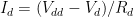
. Taking the difference of two measurements increases the noise of the measurement, and if Vdd is large enough that voltage dividers are needed, then the current through the voltage divider also goes through the load resistor, making measuring low drain currents (when Vgs is small) difficult.

The common-drain circuit only requires measuring Vg and Vs, both of which can be within the analog-to-digital converter range even when Vdd is large, assuming that the load resistor (Rs in this case) is chosen sufficiently small. Determining Vgs requires a subtraction, but Id does not. Avoiding voltage dividers (with their current stealing and the extra trouble of measuring the divider ratio) seemed like a good idea.

I tried making measurements with the common-drain configuration today, and found it surprisingly difficult. I kept getting huge amounts of noise on the Vs plot, whenever the FET was on. It appeared to be 120Hz interference, but I have no idea where the interference was coming from—the power supply did not show significant 120Hz ripple and large bypass capacitors on the power supply lines did not help. I finally managed to get rid of the problem by putting a 10µF capacitor between the source and drain, providing a negative feedback path that eliminated the problem. (The capacitor appeared to make no difference to the plots for common-source configurations.)

The common-source circuits, however, provided much cleaner plots than the common-drain circuits. The common-source circuits also allowed me to measure much higher drain currents, because I could go to a higher Vgs value without exceed the ADC range when Vs was constrained to be 0V.

For the range that I could measure, I got essentially the same current whether I measured drain current or source current, and pretty much independent of the voltage and load resistance I used. To first approximation, it looks like Id is a function of Vgs in a way that the equivalent resistance that plotted in Possible new FET lab for electronics course is not.

Using a small load resistor allows measuring up to a fairly high current (Vdd/R), as long as the power supply can deliver the current and the resistor doesn't overheat. Using a large load resistor allows measuring to a fairly low current.

Using a small load resistor allows measuring up to a fairly high current (Vdd/R), as long as the power supply can deliver the current and the resistor doesn’t overheat. Using a large load resistor allows measuring to a fairly low current.

Next Page »