Gas station without pumps

2019 January 1

Impedance tokens

Filed under: Circuits course — gasstationwithoutpumps @ 13:42
Tags: ,

I have been planning to add a little to the loudspeaker-impedance lab in BME 51B for the spring—a simpler measurement and modeling warmup using series or parallel RC circuits.  The idea is to give each group a different unknown impedance, which consists of a resistor and capacitor in series or in parallel, then have them measure the impedance with the Impedance Analyzer function of the Analog Discovery 2, and fit a model (R+C or R||C as appropriate).

The idea is to give the students a simpler warmup exercise for collecting and fitting data, before they tackle the more complicated loudspeaker model.

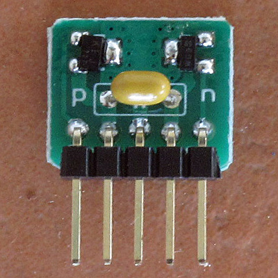
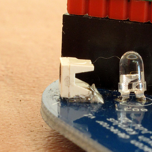
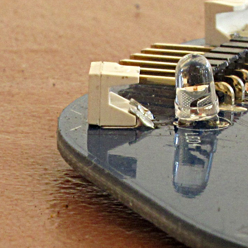
To make the unknown impedances, my son and I designed small printed-circuit boards that could take up to 6 SMD components (1206—or 3216 if you prefer the metric designation).  The components are fairly large, and so not too difficult to hand solder, and I bought an assortment of resistors and an assortment of capacitors from AliExpress to populate with.

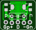
The schematic for the impedance token is designed to allow several different RC circuits—both as single impedances or as voltage dividers.

All possible 2-port, series-parallel circuits of 3 components can be wired between two adjacent pins, though three components in parallel requires adding an extra 0Ω component to get Z2||Z3||Z4 (shorting Z1). Of the 10 possible 4-component, 2-port parallel circuits, 6 can be made between adjacent pins, 2 only between pins A and C, and 2 are not achievable on the board.

With B as the center pin of a voltage divider, we can get several useful configurations:

  • Z2 paired with Z3||Z4
  • Z5+Z6 paired with Z3
  • Z5+Z6 paired with Z3||Z4
  • Z2||Z5 paired with Z3||Z4 (shorting Z6)

The board designs are available at https://users.soe.ucsc.edu/~karplus/bme51/pc-boards/ImpedanceToken/

The top shows a panel of 10 boards as delivered by Seeedstudio. The middle row has the boards after breaking apart and sanding the edges. The bottom row shows the boards populated, with heat-shrink tubing to hide the components and label the board.

I had the boards made by Seeedstudio this time (rather than SmartPrototyping), because I had a coupon code for a discount and because Seeedstudio did not charge extra for fancy colors of soldermask.  Seeedstudio had to email me to ask if I was willing to accept panelizing, while SmartProtoyping puts that question on their web form when the job is submitted.

The hole at the top of each board is for hanging the boards from hooks or putting them on a keychain—I’m going to have to do something to make sure that I get all the tokens back after each lab that uses them.

I wrote a program to generate random series or parallel RC circuits based on the components in the assortments and constraints on the range of impedance and the RC time constant. The programs are available at https://users.soe.ucsc.edu/~karplus/bme51/pc-boards/ImpedanceToken/populating_tokens/

I’ve populated 10 of the boards so far, and they all seem to be ok, except for one whose 100nF capacitor seems to be 160nF instead of 100nF. I think that this may be a labeling error on the assortment of capacitors I bought. If the others from the same strip also come out to 160nF, I’ll relabel the strip. (The capacitors themselves are not labeled, though the resistors are.)

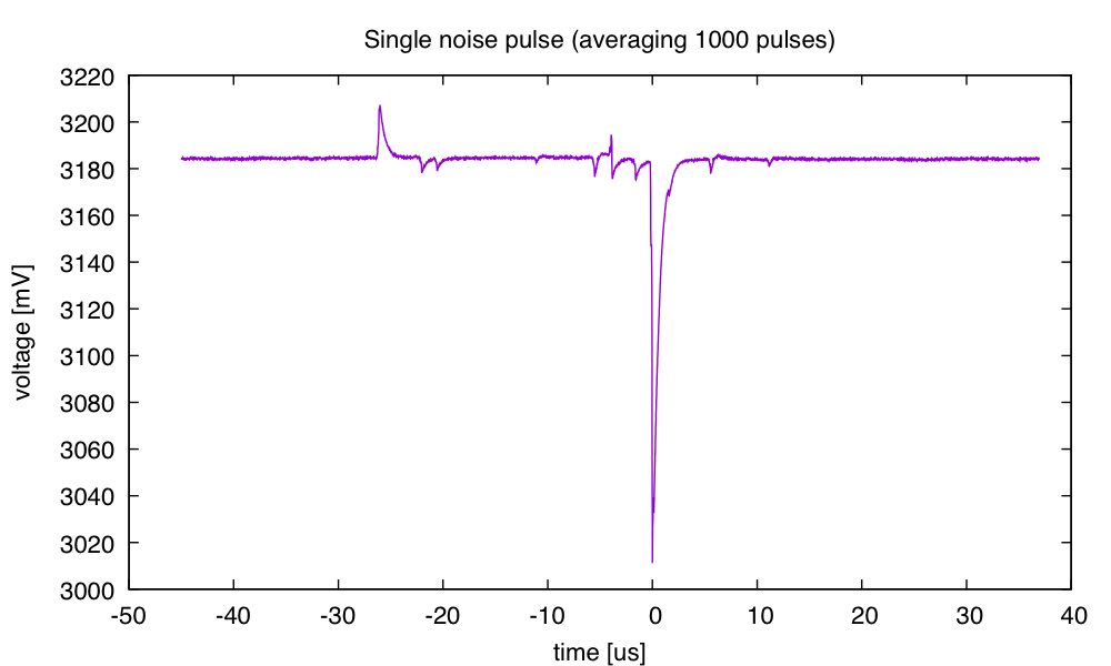
One problem I’ve found in characterizing the boards is that the screwless terminal on the adapter board for the Analog Discovery 2 impedance analyzer has its contacts recessed too deep—the header pins can’t reach the contacts.  I’ve found the screwless terminal to be more of a nuisance than timesaver, both because the contacts are recessed so deep and because the release buttons are difficult to press. I’m considering buying a 0.1″-pitch, 2-contact screw terminal to replace the screwless terminal with.

When I tried adding wires from the adapter board to a breadboard, I got inconsistent readings with about 10Ω–20Ω resistance in series with what I was measuring—I think this may have been bad contacts in either the screwless terminal or in the breadboard.  I switched to using the breadboard directly with my own reference resistor rather than using the impedance analyzer adapter board and had no further problems.


2018 January 3

SOT-23 FETs for half H-bridge

Filed under: Circuits course — gasstationwithoutpumps @ 20:53
Tags: , , , , ,

In Breakout board for SOT-23 FETs, I gave the schematic and layout pictures for a half H-bridge breakout board using SOT-23 surface-mount FETs.  The boards arrived today, 12 days after I ordered them. The boards cost $4.86 plus $23.79 shipping, but I had them panelize the design, and they sent me 13 copies instead of 10, so I ended up with 546 boards (instead of 420), making a cost of 5.24¢ each.

One of the panelized board. The panels are just separated with V cuts, so the corner rounding is not very good, but there is some, and I did not end up with sharp corners after cutting off a row of boards with tin snips.

With the transistors, capacitor, and headers, each half H-bridge will cost under 40¢ in 100s—much less than the approximately $1.37/half H-bridge that separate TO-220 FETs cost.

Today I tried soldering on a  PMV20XNER nFET (14.9¢ in 100s) and SSM3J332R pFET (12.4¢ in 100s), a 5-long right-angle header, and a 10µF ceramic capacitor. I wanted to do this with pretty much the same tools the students would have, so I did not use a board holder nor cross-lock tweezers (both of which would have made the job slightly easier).  My technique was simple:

  • Put the board face up on the bench.
  • Place one FET using sharp-pointed tweezers.
  • Tape the FET and the drain side down with a tiny piece of blue painters’ tape.
  • Solder the source and gate.
  • Remove the tape.
  • Solder the drain.
  • Repeat for the other FET.
  • Put the headers through the holes (from the component side).
  • Flip the board over and solder the header.
  • Put the header pins into a breadboard at the edge of the board.
  • Insert the capacitor from the component side.
  • Prop the breadboard up so the solder side of the board is exposed.
  • Solder the capacitor in place and trim its leads.

Soldering the first board went well.  The second one was a little harder (I had a bit of hand tremor), but still only took a few minutes.  Having made the lands huge (big enough for wave soldering) made alignment fairly simple—I did not have to be exact.

I tried one FET without the trick of taping the FET in place—that did not work at all, as the FET moved completely off the pad when I tried to solder.  I had to remove solder from the board with a solder sucker and redo the FET using tape.

Here are the front and back of the boards before and after populating, along with the pointed tweezers I used for placing the FETs.

Here is a close-up of one of the two boards I soldered (the one with the worst alignment—see the pFET at the top left).

I spent the rest of the afternoon checking that the boards were OK.  I used essentially the same setup as I used for Ron vs Vgs for pFETs and nFETS, with a 24Ω load and a 10V ramp that gradually turned the transistor off.  Because the test was the same, I plotted the results together with the old results:

The PMV20XNER transistor has a much lower threshold than the other nFETS I’ve looked at, but a comparable Ron to the other power nFETs.

The SSM3J332R pFET also has a low threshold voltage and the on resistance is in the same range as others we have used in the past.

It looks to me like the half-H-bridge will be a perfectly reasonable way for the students to get FETs for the class-D amplifier.  The current will be somewhat limited by the power dissipation of the pFET, but with an 8Ω speaker and 0.1Ω pFET, the power to the loudspeaker should be 80 times the power lost in the pFET, so the 10W limit on the loudspeaker should be reached well before the half H-bridge overheats.

Update: the EAGLE and Gerber files for this board are available at https://users.soe.ucsc.edu/~karplus/bme51/pc-boards/

2018 January 1

Robot moving, but unreliably

Filed under: Robotics — gasstationwithoutpumps @ 10:05
Tags: ,

I got some time last week to play with my uncompleted robot from the mechatronics course.  I wired up all the motor and encoder connections and wrote a short program that was supposed to move the robot in a square (forward for 12″, 90° right turn, repeat).  I did not expect it to work well—some calibration of the distances was clearly going to be needed, but I expected repeatable motion.

I got sort of repeatable motion on the wooden dining-room floor, though the angle of the turns was not right, but on the rougher tile floor in the breakfast room and kitchen it would occasionally get stuck turning in a circle with one wheel stopped and the other running forward continuously.

Diagnosing the problem was fairly simple—the count for the number of steps from the encoder of the continuously turning wheel was not increasing, so the robot thought that no progress was being made and kept running that motor, while slowing down the motor whose count was still increasing until that motor stopped (near the target number of counts).  The reason that the count was not increasing was that the connector from the encoder to the PC board was shaking loose—pressing the connection sideways would often restore the counting and return the robot to its advance-and-turn behavior.

Fixing the problem is more difficult.  I had crimped female headers onto the wires from the motor and encoders to the PC board, and even put a little solder in the crimped joint, because the 28-gauge stranded wires did not work well with the crimped headers.  The connection failure now seems to be between the male header pins and the female crimp-on connector, which is hard to do much about.

The short wires from the motor and encoders are on a 6-pin 2-mm-pitch female connector (similar to the JST PH connector, though probably not a brand-name connector—that connector seems to be made by all the major connector manufacturers and knockoffs made in China are common). I can get cheap cable assemblies for such connectors, with either bare wire ends (as came with the motor) or with the female connector on both ends of the cable.  Because the pitch is 2mm, rather than 2.54mm, such connectors are not usable with breadboards or perfboards.

I’m now facing two choices:

  • Solder the motor/encoder cables to my perfboard, rather than using the failing header-pin connections.
  • Make a custom PC board for the motor controller with the 6-pin 2mm-pitch connectors for pluggable connections.

The soldering would be a quick fix, at least until the thin wires broke, but is a bit of a pain, as my power board was crammed rather tight. The PC board is a better long-term option, but I need to look ahead to all the different things I might want the robot to do, as it will be difficult to rewire or reassign pins with a PC board.  If I do a PC board, I again have two options:

  • Do a motor-controller-only PC board, with 4-pin or 6-pin headers to the existing processor board.
  • Put the processor, motor-controller, and interface electronics all on one mother board, with cable connections to the sensors.

The combined board would reduce the cabling and number of connectors that might fail, as well as taking up less total space (on-board connections are much more compact than connectors and cables), but I’d need to figure out what I want to do with all the pins of the Teensy 3.2, as adding connections later would be tough, unless I allowed for expansion now.

If I’m going to do a custom PC board, I should do it this week, before classes start, as I’ll be spending all my time on the applied electronics course (lecturing, running labs, and grading) once the quarter starts.

The vibration on the rough surface of the tile floor also revealed another problem for the robot—the M3 bolts (machine screws) that held the bumper on vibrated loose, resulting in the bumper drooping and getting caught on my sleeve when I picked the robot up.  The bumper then cracked at the narrowest part.  I need to get some M3 lock nuts, I think, and redesign the bumper to be a little more robust.  Unfortunately, I no longer have access to the labs that have SolidWorks installed (turned off when all the student access to the labs was turned off), though I still have access to the laser cutter—I may have to request access again.

Incidentally, AliExpress recently sent me a suggestion for a slightly better way to connect the bumper switches: https://www.aliexpress.com/item/Endstop-Mechanical-Limit-Switches-3D-Printer-Switch-for-RAMPS-1-4-Free-Shipping-Dropshipping/32640551085.html. These switches are mounted on a PC board with a sturdy connector and an LED that lights up when the switch is pressed.  Unfortunately, the 3-wire connection they use does not follow the standard used for servo wiring, as they put the positive connection on the outside and the GND in the middle, swapping these two wires.

2017 December 22

Breakout board for SOT-23 FETs

Filed under: Circuits course — gasstationwithoutpumps @ 23:25
Tags: , , , , , ,

After a discussion in the comments of Ron vs Vgs for pFETs and nFETS with Michael Johnson, I decided to design my own breakout boards for SOT-23 surface-mount FETs, with the possible use of them in the class-D amplifier lab in place of the through-hole TO-220 FETs we’ve been using.

I picked a couple of 30V FETs (one nFET, one pFET) whose data sheets indicated that they would have adequately low on-resistance with a gate voltage of only 2.5V (–2.5V for the pFET), so that the FETs could be controlled by a 3.3V logic signal with no problems.  I ended up picking PMV20XNER for nFET (14.9¢ in 100s) and SSM3J332R for pFET (12.4¢ in 100s).

Although the drain-to-source voltage is allowed to go to 30V, the gate-to-source voltage is more limited (±12V for both the nFET and the pFET).  That should be adequate for anything we do in the course, as our maximum power supply is ±5V, so we shouldn’t see any voltage differences bigger than 10V.  (I could have saved a few cents by using 20V FETs instead of 30V ones, maybe.)

Because the students use the FETs in an H-bridge, I decided to make my breakout board be a half H-bridge, with an nFET, a pFET, a bypass capacitor, and 5 right-angle header pins:

The schematic is quite simple. (The diodes are the body diodes of the FETs.)

The layout took me a while, because I wanted to make as much heat sinking as I could get on a small, cheap board.  The standard footprint for a ST-23 allows a thermal resistance of about 120 K/W. I did not push too hard though, because even with ideal layout, the SOT-23 packages still have terrible thermal conductivity (about 90 K/W)—essentially all the heat is being conducted through the thin drain pin.  (The SSM3J332R reports even worse numbers: 300 K/W with minimum footprint and 120 K/W with a square inch of copper.)

Solder side of the board. Visualization provided by https://gerber-viewer.easyeda.com/

Component side of the board. Visualization provided by https://gerber-viewer.easyeda.com/

My board is not nearly a square inch of copper—the entire board is only 15mm × 12.5mm, and only half of that is used for heatsinking the drains. I used the back of the board for radiating heat and provided thermal vias around the drain pads to connect the front and back. The footprint for the pads is one provided by the manufacturers for wave soldering—I thought it would be easier for had soldering than the much smaller pads used for reflow soldering.

The gate connections are on the outside, the source connections just inboard of them, and the shared drain in the middle.  The board is basically symmetric with respect to nFET and pFET, but I labeled the two sides so that there would be less variation in how students soldered them up.

The bypass capacitor is close to the FETs (much closer than the students ever got on a bread board), so we should see less noise injection back into the power rails than we’ve seen in the past. The resistance of the source and drain traces adds another 5mΩ of resistance to the H-bridge, which is not too bad—the beardboard probably adds more like 50mΩ.

If I understood their website correctly, I should be able to get 10 copies of the tiny board panelized in a 6×7 array (so 420 boards after I cut them apart) for only $4.90 from Smart-Prototyping.com.  Of course, I’m in a hurry, so I ended up paying an extra $23.79 for shipping with DHL, so the order costs $28.69, or <7¢ a board.  I also ordered 10 40-pin right-angle male headers (enough for 80 boards) for $4.11 from AliExpress, raising the price to 12¢ a board.

With the transistors, each half H-bridge will cost under 40¢ in 100s—much less than the approximately $1.37/half H-bridge that the separate TO-220 FETs cost.

The difference in cost is not important for the course ($2 a student), so my main consideration is whether the students will learn more by doing some surface mount soldering with a fixed cMOS half-H-bridge design or by continuing to wire up separate transistors on the bread board (making the usual student errors of getting the pinout wrong or general miswiring).  There is still plenty of room for error on the half H-bridge: swapping transistors, getting 2 nFET or 2 pFET instead of one of each, putting the whole board in backwards to short the power supply through the body diodes, …. .

The SOT-23s can’t dissipate quite as much heat as the TO-220s, but we’ll probably not have much heat to dissipate in reasonable designs.  With a 5V supply, 8Ω load, and 73mΩ on-resistance, the power dissipation in the pFET should be only about 28mW and the nFET even less—way less than the 500mW or so that I expect the boards to be able to handle.  Shoot-through current is mainly what the students will need to worry about, as that can get quite high with the low on-resistances of both the nFET and the pFET.

I’ve ordered the boards and parts to test out using the SOT-23 FETs and half-H-bridge boards.  If they work out well, I’ll probably rewrite the class-D lab to have students do a little surface-mount soldering (SOT-23s are about the simplest intro).

2017 August 6

Beacon detector board

I’m planning to sit in on CMPE 118/L (Mechatronics) this fall, and so I started looking over some of the material for the course from previous years.  One exercise involved designing a “beacon detector” that signals when it sees an infrared signal modulated with a 2kHz square wave. The exercise calls for an all-analog solution (phototransistor, transimpedance amplifier, active filter, rectifier, peak detector, …), which I plan to do when the time comes, but I got intrigued by the idea of doing an almost purely digital design.  That was the motivation for the Goertzel filter blog post.

I decided to take the digital design further and make a beacon detector that not only detects the 2kHz IR beacon, but also indicates what direction it is in.  To do this, I wanted 8 phototransistors around a circle, with one every 45°.  One can get a crude estimate of the angle from just which detector gets the strongest signal, but with wide-angle sensors one should be able to get finer estimates by looking at the ratio of the signals from two adjacent channels.

Because I was deliberately going for minimal analog design as an exercise, I used just a phototransistor and a pullup resistor for each channel, and a Teensy LC board for all the processing.  I chose SFH325FA side-look phototransistors, because they provide a nice, cubical package that I thought would make them easier to align.  They are surface-mount components, but with a 2.54mm pitch for the two terminals, they aren’t much harder to solder than through-hole parts.

For testing, I soldered one of the SFH325FA phototransistors to a pair of male header pins. This allowed me to experiment with different pullup resistor sizes in different lighting conditions and at different distances from an IR emitter.

My experimentation with different pullup resistors indicated that I could not operate in full sunlight, no matter what size pullup resistor I used—when the pullup was small enough that the phototransistor had sufficient voltage across it in full sunlight, the signal from the IR beacon was too small to be useful.  With AC-coupled amplifiers, I could have made it work, but I was committed to nearly pure digital solution.  If I had sunlight nearby, but the phototransistor itself was shaded, then I could go up to 22kΩ for the pullup without problems. The limiting factor was then that a very close beacon could saturate the detector, making it hard to determine power ratios.  I ended up choosing 22kΩ as my pullup, as I wanted to detect beacons from up to 2m away.

With a 22kΩ pullup and a strong signal, I can get a very clean “shark’s fin” waveform, because of the capacitance of the phototransistor acting with the resistor as a low-pass filter.  This low-pass filtering helps remove aliasing artifacts from the sampling by the analog-to-digital filter.

Behind each phototransistor I placed an LED, to indicate which channel had the maximum signal.  I charlieplexed the LEDs, so that I needed only 4 I/O pins for the 8 LEDs (I could encode up to 12 LEDs with 4 charlieplex wires). I used WP710A10SGC green LEDs for the indicators, because I had a lot of them around, but it would have been better to use an amber LED with a wide-angle, diffuse case, as the green indicators are only clearly visible over a fairly narrow angle.  The current-limiting resistors I used would keep the current low enough even with a low-forward-voltage red LED.

I also added an RGB LED to indicate the overall state—I used a common-anode one, because my son had a lot of them with diffuse cases, which are best for an indicator that needs to be seen from any angle.  The RGB LEDs were part of an unidentified lot from China, so I don’t have a part number or specs for them.  I hooked them up to PWM pins, so that I could adjust the brightness and color as needed.

I also designed in a connector for SPI connection, so that the board could be used a slave peripheral of another microcontroller.  I used Eagle on my old laptop to design the PCB (I know that in Need to find new PC board software and PCB CAD tools I said that I would be trying to switch to KiCAD or Diptrace, but I was lazy and stuck with what I already knew how to use).

I sent the design to Seeedstudio to make the PCB—like many of the Chinese firms that cater to hobbyists, they had a sale in July of boards up to 10cm×10cm for only $5.  Of course, it cost me another $21 for shipping with DHL, because I was too impatient to wait for Chinese air mail (and not trusting enough of the reliability). I chose Seeedstudio because they had the best user interface to their design-rule check, and at least as good pricing as anyone else.

The boards arrived quite quickly—only 8 days from order to delivery. Here is what they look like:

The back of the board has some documentation to remind me what is connected where.

The front of the board has relatively little documentation.

The boards are 8cm×8cm, fitting comfortably within both the cheap manufacturing limit and the Eagle free-version size limit.  I made them this big so that the Teensy LC board would fit without interfering with mounting holes (for M2 and M3 screws) and a central hole for attaching the board to a servo arm.

Getting a good right angle for the surface-mount phototransistors took some practice:

My first solder joint for the SFH325FA phototransistor tilted the transistor substantially, because the solder underneath formed a wedge. I reworked it a couple of times and finally got something sort of acceptable.

By the fifth phototransistor, I had worked out a technique that seemed to hold the phototransistor cleanly at a right angle. There is probably not much solder underneath the phototransistor, but the large wedge behind the phototransistor should provide sufficient mechanical strength.

Here are pictures of the populated board:

The back of the board does not look very different after being populated. I put one M3 screw in the bottom M3 screw hole, in order to see how compatible the screw hole design is with the screw head.

The top of the board, when populated shows how close channels 0 and 7 come to the Teensy board.

Here the board is on (powered through the USB cable), detecting an IR beacon about a meter away in the direction of channel 4. The green LED by the channel indicates the direction, and the green RGB LED indicates a strong signal.

I put the header pins on the pullup resistors, so that I could record the signal seen by the analog-to-digital converters.  Unfortunately, the signal is much noisier than I expected:

The large spikes are at 15kHz, and probably correspond to noise injected by the ADC sampling.

I turned off the beacon and looked just at the noise spikes, using the 10× probe on the oscilloscope to get better bandwidth.  I sampled at 100MHz and averaged 1000 traces to get a clean view of the signal (the triggering was set far enough from the background level that only fairly large spikes were captured, but close enough that the 1000 frames were gathered as quickly as possible).

The pulses are very short (2–3 µs), so almost certainly correspond to the charging of the sampling capacitor. After looking at this waveform, I changed my sample time on the ADC to 2µs (it had been 1µs) to reduce the noise in what the ADC reports.

This post has gotten more than long enough, though I still have a couple of things that should be added: a schematic diagram of the board and a plot of the reported angle vs actual angle.

The schematics from Eagle are really ugly, so I’ve been thinking about redrawing them with SchemeIt—perhaps that can be a subsequent post.

The reported angle vs. actual angle plot is going to require building a jig that allow me to set the angle precisely.  I tried jury-rigging something out of Lego today, but the result had too much slop—the board could not be reliably set level with the IR emitter at a fixed angle.  The OED-EL-1L2 5mm IR emitter does fit in the middle hole of a Lego Technic brick, so I using Lego to align the IR emitter was attractive. I may have to make something out of wood and MDF (medium-density fiberboard) for a more solid test jig.  The M3 screw holes will allow me to attach the board firmly to MDF with standoffs, and I can drill holes in Lego bricks to make a stand for the IR emitter.


Next Page »